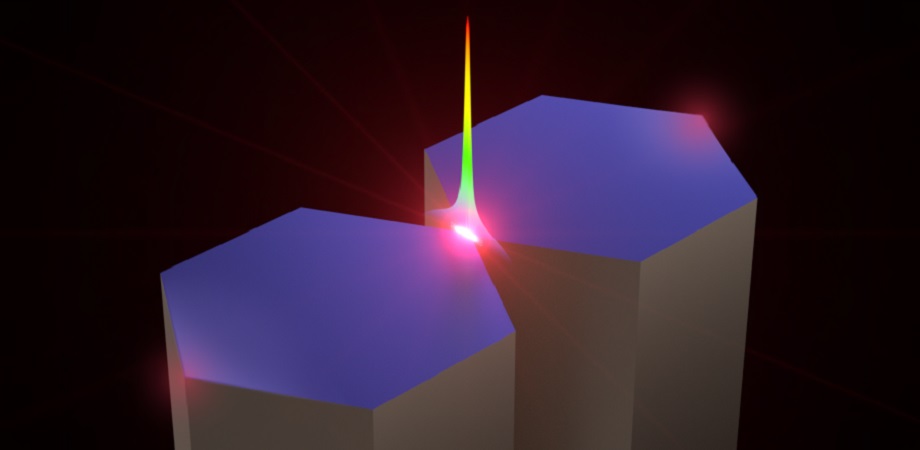
Light is extremely confined in a nanoslit in a coupled-nanowire-pair. Image courtesy of Zhejiang University Nanophotonics Group led by Limin Tong.
Imagine shrinking light down to the size of a tiny water molecule, unlocking a world of quantum possibilities. This has been a long-held dream in the realms of light science and technology. Recent advancements have brought us closer to achieving this incredible feat, as researchers from Zhejiang University have made groundbreaking progress in confining light to subnanometer scales.
Traditionally, there have been two approaches to localize light beyond its typical diffraction limit: dielectric confinement and plasmonic confinement. However, challenges such as precision fabrication and optical loss have hindered the confinement of optical fields to sub-10 nanometer (nm) or even 1-nm levels. But now, a new waveguiding scheme reported in Advanced Photonics promises to unlock the potential of subnanometer optical fields.
Picture this: light travels from a regular optical fiber, embarking on a transformative journey through a fiber taper, and finding its destination in a coupled-nanowire-pair (CNP). Within the CNP, the light morphs into a remarkable nano-slit mode, generating a confined optical field that can be as tiny as a mere fraction of a nanometer (approximately 0.3 nm). With an astonishing efficiency of up to 95 percent and a high peak-to-background ratio, this novel approach offers a whole new world of possibilities.

Waveguiding scheme to generate a sub-nm-confined optical field in a nano-slit mode. (a) Schematic illustration of the CNP waveguiding scheme. (b) 3-D plot of the cross-sectional field intensity distribution of the nano-slit mode. Credit: Yang, Zhou, et al., doi 10.1117/1.AP.5.4.046003
The new waveguiding scheme extends its reach into the mid-infrared spectral range, pushing the boundaries of the nano-universe even further. Optical confinement can now reach an astonishing scale of approximately 0.2 nm (λ/20000), offering even more opportunities for exploration and discovery.
Professor Limin Tong of the Zhejiang University Nanophotonics Group notes, “Unlike previous methods, the waveguiding scheme presents itself as a linear optical system, bringing a host of advantages. It enables broadband and ultrafast pulsed operation and allows for the combination of multiple sub-nanometer optical fields. The ability to engineer spatial, spectral, and temporal sequences within a single output opens up endless possibilities.”
The potential applications of such breakthroughs are awe-inspiring. An optical field so localized that it can interact with individual molecules or atoms holds promise for advancements in light–matter interactions, super-resolution nanoscopy, atom/molecule manipulation, and ultrasensitive detection. We stand at the precipice of a new era of discovery, where the tiniest realms of existence are within our grasp.
Check out the video summary with an animated demonstration from the authors:
Read the Gold Open Access article by L. Yang, Z. Zhou, et al., “Generating a sub-nanometer-confined optical field in a nanoslit waveguiding mode,” Adv. Photon. 5(4), 046003 (2023), doi 10.1117/1.AP.5.4.046003