
Oksana Semenova, Aleksei Sosunov, Nikolai Prokhorov, Roman Ponomarev, "Temperature dependence of LiNbO3 dislocation density in the near-surface layer," Chin. Opt. Lett. 20, 061601 (2022)
- Chinese Optics Letters
- Vol. 20, Issue 6, 061601 (2022)
Abstract
Keywords
1. Introduction
Lithium niobate (
For all these applications, the important role is not of the bulk properties of LN but of its near-surface layer, because the ridge or buried waveguides and electrodes are created on the surface of the crystal. Some authors[
It is well known that electro-optical properties of LN are sensitive to the intrinsic defects and impurities. Structure defects in LN crystals can be roughly divided into two types: internal, related to the crystal growth, and external, related to the wafer dicing and polishing. The defect structure of a congruent LN consists of Li vacancies,
Sign up for Chinese Optics Letters TOC. Get the latest issue of Chinese Optics Letters delivered right to you!Sign up now
External or technological defects arise during the cutting and polishing of LN. Despite the high quality of the optical surface, which is obtained during cutting and polishing, the number of defects increases[
The structure of the damaged near-surface layer in LN has a deformation nature with the multiplication of the dislocation density[
The aim of this work is to analyze experimentally and theoretically the dislocation density of the near-surface layer of LN as a function of the thermal annealing temperature.
2. Materials and Methods
The samples used for the investigations were congruent X-cut LN 1-mm-thick wafers by Fomos Materials (Russia). The wafers were cut into
Thermal annealing (treatment) of LN was performed at temperatures of 400°C, 500°C, and 600°C in air atmosphere. The samples were heated by 10°C/min to the required temperature, then for 4 h they were annealed, and after that they were slowly cooled in the furnace. In addition, there was a reference sample without annealing. Thermal annealing is required to reduce internal stresses, absorption[
The dislocation density on the surface of LN was estimated by the method of identifying etching pits by using wet selective etching in the melt of KOH with 35% NaOH for 5 min at a temperature 200°C. Detection of etching pits was carried out using the optical microscope Leica DMi8 in reflected light and a bright field. All samples were cleaned sequentially in isopropyl alcohol and distilled water for 3 min in an ultrasonic bath.
The topology of the etch pits was studied using atomic force microscopy (AFM) in the semi-contact mode (NT-MDT NTEGRA Prima Corp.). Analysis and quantitative calculation of AFM images were carried out using the program Nova 1.1.1 NT-MDT.
The dislocation density was also experimentally estimated using the X-ray method based on the account of an extinction effect in imperfect single crystals, using a model of randomly distributed dislocations. X-ray diffraction (XRD) was carried out by using a precise double-crystal spectrometer. The monochromator was a dislocation-free Si crystal, set in the position corresponding to the reflection
3. Results
3.1. Wet selective etching
The real structure of LN was revealed by the wet selective etching method, which can be used to analyze the dislocation density. Many etching pits appear on the surface with selective etching, which are the emergence of dislocations caused by cutting and grinding of a monocrystalline wafer. Also, the authors[
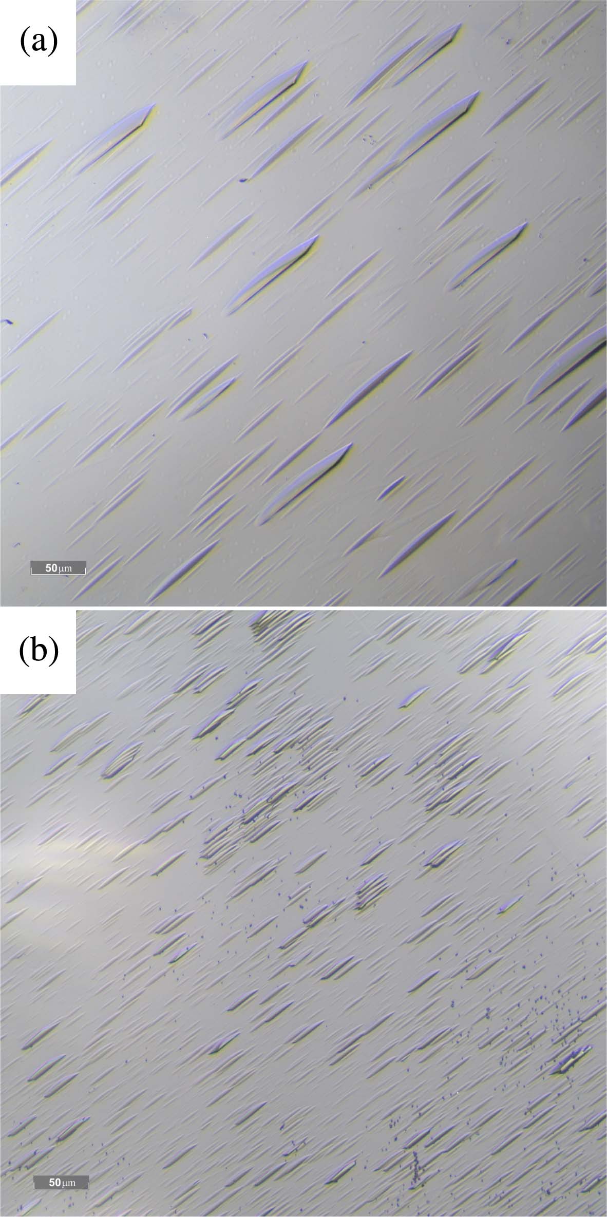
![]()
Figure 1.Etching pits of LiNbO3 (a) after thermal annealing at 500°C and (b) in pristine state.
The near-surface layer of the crystal was treated by thermal annealing to reduce the density of dislocations and stresses. The dislocation etching pits on the surface before and after thermal annealing were detected with an optical microscope (Fig. 1). The calculated dislocation density
![]()
Figure 2.Dependence of the dislocation density N determined by wet selective etching on the annealing temperature T.
For determination of the etching depth some samples were studied using AFM. The distribution profiles of the pits by their depth were obtained. One of these profiles is shown in Fig. 3. The etching pit depth varies from 5 to 100 nm. This means that the etching rate is from 1 to 20 nm/min.
![]()
Figure 3.AFM image of etch pits and the profile of etching pits (line 146).
3.2. X-ray diffraction results: theory and experiment
When considering XRD on single crystals, it is necessary to take into account the dynamic extinction effects, which lead to a decrease in the integral reflection coefficients
The value of
The radiation scattered by kinematic volumes is incoherent among instances and with the radiation scattered by the rest of the (dynamic) crystal. Then, the integral component of the reflection of the crystal volume is equal to
Considering the two types of polarization
Here,
Therefore, an integral reflection coefficient and an extinction parameter are equal to
The value of
In the case of Bragg’s angle, the extinction depth is[
Here,
The part of the kinematic volume
For X-cut samples, the observation plane of etching pits
These Burgers vectors are located on the basis plane (0111), i.e., it should be considered for a Z-cut. Therefore, we will consider the sliding directions
Calculating the weight factor
An expression of the integral reflection coefficients
Here, the index “(1)” refers to the first-order reflections (110), and the index “(2)” refers to the second-order reflections (220),
Equation (10) allows us to construct a theoretical dependence of the ratio of the integral reflection coefficients corresponding to two reflection orders to the density of chaotically distributed dislocations, shown in Fig. 4. To determine the density of dislocations in single crystals, the left branch of the presented curve should be used. That is because LN is a brittle material in which it is impossible to create conditions corresponding to large dislocation densities during plastic deformation.
![]()
Figure 4.Dependence of ρ110/ρ220 for a single crystal of X-cut LN on the density of chaotically distributed dislocations N, X-ray Co-λβ-radiation.
Table 1 shows the results of measuring the ratio of integral reflection coefficients corresponding to two reflection orders for the studied samples of different manufacturers. Using the results shown in Table 1 and the calculated curve
![]()
Figure 5.Dependence of the dislocation density N (determined by the results of XRD) on the thermal annealing temperature T.
| Thermal Annealing | Sample |
|---|---|
| Pristine | 3.17 |
| 400°C – 4 h | 3.26 |
| 500°C – 4 h | 3.57 |
| 600°C – 4 h | 3.55 |
Table 1. The Experimental Ratio of the Integral Reflection Coefficients
4. Discussion
Dislocations characterize the imperfect structure of materials. In this paper, we present results of dislocation density measurement in
It is known that etching pits do not cover all surface areas of the wafer, but are located in positions where dislocations appear[
Figure 1 shows the decrease in the density of etching pits for treated samples and an increase in their size at a temperature of 500°C. These pictures were chosen because the thermal annealing temperature of 500°C is the most optimal and demonstrates minimum density of etching pits (see Fig. 2). The increase in linear size of etching pits in Fig. 1(a) can be explained by the duration of etching. But, the experimental conditions had to be identical. The etching pits were not ranked by size while being counted. The number of pieces per unit area was counted directly.
A slight increase in the number of defects at 600°C (Fig. 5) indicates the beginning of deformation processes associated with the restructuring of the LN crystal lattice due to the high mobility of the ions at high temperatures. The X-ray method for determining the dislocation density is based on the measurement of integral intensity of the reflection lines of two orders. It is known that the integral intensity is affected by any change in the crystal structure[
Note that etching of single crystals makes it possible to estimate the density of defects on the surface of studied images, and the second method using the X-ray allows the estimation of the density of dislocations to be distributed over the depth of the samples. The volume was determined by the penetration depth of the X-rays. In our case, this was of the order of 15 µm, which is approximately equal to the depth of the defect layer, as reported earlier[
In addition, we note that the proposed extinction model of crystals with random dislocation distribution allows us to measure dislocation density ranging from
Thus, the treatment of LN crystals repairs the damaged layer by reducing the density of dislocations. These results are most important from the point of view of increasing the homogeneity of the structure of the near-surface layer and formation of more stable optical waveguides, integrated-optical circuits, and LNOI components/devices. For example, the creation of ridge waveguides for LNOI is performed by diamond blade dicing with subsequent polishing[
5. Conclusion
This work is dedicated to the study of the dislocation density of the near-surface layer of X-cut LN crystals, depending on thermal annealing in the range of 400°C–600°C.
Firstly, the experimental method of wet selective etching was applied to determine the dislocation structure of LN before and after treatment. Secondly, a method was proposed to determine the dislocation density by using XRD based on the account of the extinction effect in imperfect single crystals, using a model of randomly distributed dislocations (theory and experiment). These two methods were used to analyze the dislocation structure of crystals. This is enough to establish a relation between the treatment and the real structure of the LN crystal. It has been experimentally proved that thermal annealing of LN samples at a temperature of 500°C is accompanied by a decrease in the density of dislocations in the near-surface layer.
The obtained results are applicable to other optical materials as well. In addition, the found LN treatment regimen can improve the properties of Ti-diffused, proton-exchanged, and ridge waveguides for various optical systems.
References
[1] A. Boes, B. Corcoran, L. Chang, J. Bowers, A. Mitchell. Status and potential of lithium niobate on insulator (LNOI) for photonic integrated circuits. Laser Photonics Rev., 12, 1700256(2018).
[2] K. Noguchi. Broadband Optical Modulators: Science, Technology, and Applications(2012).
[3] M. N. Armenise, C. Ciminelli, F. Dell’ Olio, V. M. N. Passaro. Advances in Gyroscope Technologies(2011).
[4] A. V. Turutin, J. V. Vidal, I. V. Kubasov, A. M. Kislyuk, D. A. Kiselev, M. D. Malinkovich, Y. N. Parkhomenko, S. P. Kobeleva, A. L. Kholkin, N. A. Sobolev. Highly sensitive magnetic field sensor based on a metglas/bidomain lithium niobate composite shaped in form of a tuning fork. J. Magn. Magn. Mater., 486, 165209(2019).
[5] P. Chaudhary, H. Lu, A. Lipatov, Z. Ahmadi, J. P. V. McConville, A. Sokolov, J. E. Shield, A. Sinitskii, J. M. Gregg, A. Gruverman. Low-voltage domain-wall LiNbO3 memristors. Nano Lett., 20, 5873(2020).
[6] D. Sun, Y. Zhang, D. Wang, W. Song, X. Liu, J. Pang, D. Geng, Y. Sang, H. Liu. Microstructure and domain engineering of lithium niobate crystal films for integrated photonic applications. Light Sci. Appl., 9, 197(2020).
[7] B. Zhang, L. Wang, F. Chen. Recent advances in femtosecond laser processing of LiNbO3 crystals for photonic applications. Laser Photonic Rev., 14, 1900407(2020).
[8] L. Carletti, A. Zilli, F. Moia, A. Toma, M. Finazzi, C. Angelis, D. N. Neshev, M. Celebrano. Steering and encoding the polarization of the second harmonic in the visible with a monolithic LiNbO3 metasurface. ACS Photonics, 8, 731(2021).
[9] W. Lu, Z. Gao, X. Liu, X. Tian, Q. Wu, C. Li, Y. Sun, Y. Liu, X. Tao. Rational design of a LiNbO3-like nonlinear optical crystal, Li2ZrTeO6, with high laser-damage threshold and wide mid-IR transparency window. J. Am. Chem. Soc., 140, 13089(2018).
[10] S. Sanna, G. Schmidt. LiNbO3 surfaces from a microscopic perspective. J. Phys. Condens. Matter., 29, 413001(2017).
[11] R. Bhatt, I. Bhaumik, S. Ganesamoorthy, R. Bright, M. Soharab, A. K. Karnal, P. K. Gupta. Control of intrinsic defects in lithium niobate single crystal for optoelectronic applications. Crystals, 7, 23(2017).
[12] P. Galinetto, M. Marinone, D. Grando, G. Samoggia, F. Caccavale, A. Morbiato, M. Musolino. Micro-Raman analysis on LiNbO3 substrates and surfaces: compositional homogeneity and effects of etching and polishing processes on structural properties. Opt. Lasers Eng., 45, 380(2007).
[13] M. Gruber, A. Leitner, D. Kiener, P. Supancic, R. Bermejo. Incipient plasticity and surface damage in LiTaO3 and LiNbO3 single crystals. Mater. Des., 153, 221(2018).
[14] A. V. Sosunov, A. B. Volyntsev, K. B. Tsiberkin, V. A. Yuriev, R. S. Ponomarev. Features of structure and mechanical properties LiNbO3. Ferroelectrics, 506, 24(2017).
[15] J. Piecha, A. Molak, U. Breuer, M. Balski, K. Szot. Features of surface layer of LiNbO3 as-received single crystals: studied in situ on treatment samples modified by elevated temperature. Solid State Ion., 290, 31(2016).
[16] A. A. Anikiev, N. V. Sidorov, M. N. Palatnikov, M. F. Umarov, E. N. Anikieva. Parametrization of nonstoichiometric lithium niobate crystals with different states of defectivity. Opt. Mater., 111, 110729(2021).
[17] A. Sosunov, R. Ponomarev, O. Semenova, I. Petukhov, A. Volyntsev. Effect of pre-annealing of lithium niobate on the structure and optical characteristics of proton-exchanged waveguides. Opt. Mater., 88, 176(2019).
[18] Ya. A. Kosenok, V. E. Gaishun, O. I. Tyulenkova, V. G. Denisman. Aqueous compositions based on nanosized silica particles for chemical-mechanical polishing of silicon wafers. PFMT, 3, 26(2014).
[19] Y. Li, J. Lu, X. Xu. Phase transformation of monocrystalline silicon induced by polishing with diamond abrasives. IEEE Trans. Semicon. Manuf., 28, 153(2015).
[20] Ya. A. Kosenok, V. E. Gaishun, O. I. Tyulenkova. Investigation of the near-surface damaged layer in monocrystalline silicon wafers after chemical-mechanical polishing. PFMT, 4, 25(2018).
[21] Y. Li, T. Lan, D. Yang, M. Xiang, J. Dai, Z. Wang, C. Li. Research of selective etching in LiNbO3 using proton-exchanged wet etching technique. Mater. Res. Express, 7, 056202(2020).
[22] M. Leidinger, K. Buse, I. Breunig. Influence of dry-oxygen-annealing on the residual absorption of lithium niobate crystals in the spectral range from 500 to 2900 nanometers. Opt. Mater. Express, 6, 264(2016).
[23] T. Volk, M. Wohlecke. Lithium Niobate: Defects, Photorefraction and Ferroelectric Switching(2008).
[24] Z. W. Zhong. Recent advances in polishing of advanced materials. Mater. Manuf. Process., 23, 449(2008).
[25] K. Nassau, H. J. Levinstein, G. M. Loiacono. Ferroelectric lithium niobate. 1. Growth, domain structure, dislocations and etching. J. Phys. Chem. Solids, 27, 983(1966).
[26] Z. G. Pinsker. Dynamical Scattering of X-Rays in Crystals(1978).
[27] A. N. Ivanov, P. Klimanek, A. M. Polyakov. Extinction study of dislocations (Bragg diffraction). Mater. Sci. Forum, 321–324, 87(2000).
[28] A. Nakamura, J. Nakamura, I. Kishida, Y. Yokogawa. Dislocation structure at a {1¯21¯0}/〈101¯0〉 low-angle tilt grain boundary in LiNbO3. J. Mater Sci., 47, 5086(2012).
[29] K. Sangval. Etching of Crystals: Theory, Experiment, and Application(1987).
[30] J. Zhao, X. Jiao, Y. Ren, J. Gu, S. Wang, M. Bu, L. Wang. Lithium niobate planar and ridge waveguides fabricated by 3 MeV oxygen ion implantation and precise diamond dicing. Chin. Opt. Lett., 19, 060009(2021).


Set citation alerts for the article
Please enter your email address

© Copyright 2018-2021 | Chinese Laser Press. All Rights Reserved 沪ICP备15018463号-20