1Beijing Academy of Quantum Information Sciences, Beijing, China
2Division of Physics and Applied Physics, School of Physical and Mathematical Sciences, Nanyang Technological University, Singapore, Singapore
3School of Materials Science and Engineering, Peking University, Beijing, China
4Research Center for Wide Gap Semiconductor, Peking University, Beijing, China
5Key Laboratory for Physical Electronics and Devices of the Ministry of Education & Shaanxi Key Laboratory of Information Photonic Technique, School of Electronic Science and Engineering, Faculty of Electronic and Information Engineering, Xi’an Jiaotong University, Xi’an, China
6Department of Physics, College of Physical Science and Technology, Xiamen University, Xiamen, China
7CNR NANOTEC, Campus Ecotekne, Lecce, Italy
8State Key Laboratory of Low-Dimensional Quantum Physics and Department of Physics, Tsinghua University, Beijing, China
9Frontier Science Center for Quantum Information, Beijing, China
10Beijing Innovation Center for Future Chips, Tsinghua University, Beijing, China
The quest for realizing novel fundamental physical effects and practical applications in ambient conditions has led to tremendous interest in microcavity exciton polaritons working in the strong coupling regime at room temperature. In the past few decades, a wide range of novel semiconductor systems supporting robust exciton polaritons have emerged, which has led to the realization of various fascinating phenomena and practical applications. This paper aims to review recent theoretical and experimental developments of exciton polaritons operating at room temperature, and includes a comprehensive theoretical background, descriptions of intriguing phenomena observed in various physical systems, as well as accounts of optoelectronic applications. Specifically, an in-depth review of physical systems achieving room temperature exciton polaritons will be presented, including the early development of ZnO and GaN microcavities and other emerging systems such as organics, halide perovskite semiconductors, carbon nanotubes, and transition metal dichalcogenides. Finally, a perspective of outlooking future developments will be elaborated.
Microcavity exciton polaritons are hybrid quasiparticles resulting from the quantum superposition of excitons and cavity photons inside semiconductor cavities[1]. As half-light, half-matter quasiparticles, they inherit all the advantages from their excitonic and photonic components, such as low effective mass, strong nonlinearity, fast propagation, as well as enhanced sensitivity to external stimuli, such as electric and magnetic fields. These advantages allow them to be an exceptional connecting bridge between condensed matter and photonic systems, which plays important roles in not only fundamental sciences but also novel optoelectronic and quantum applications[2]. In terms of fundamental physics, as interacting bosons with low effective masses, exciton polaritons are ideal candidates for investigating room temperature collective phenomena[3], such as non-equilibrium Bose–Einstein condensation[4], superfluidity[5,6], and quantum vortices[7]. With the advances of potential trapping in polariton systems[8], exciton polaritons can be trapped to serve as artificial atoms, opening a way to effectively emulate electron Hamiltonians. This unique property generally allows exciton polaritons to be a solid-state analog of cold atoms in optical lattices, which have been shown to play important roles in topology and proposed quantum simulators with room temperature operation. In addition, being intrinsically lossy due to the limited lifetimes of their components, exciton polaritons are also promising platforms for the investigation of rich non-Hermitian physics and related applications[9,10]. In the quest for practical applications, possessing spontaneous coherence in the condensation process, exciton polaritons allow realizing polariton lasers with thresholds orders of magnitude lower than that of conventional photonic lasers, because of the exemption of the population inversion process[11,12]. In addition, due to the strong nonlinearity from their excitonic components, exciton polaritons are excellent building blocks for developing all-optical ultrafast switches and transistors[13–15], which lays the foundation for all-optical circuits[16] and chips. This strongly interacting nature also allows to induce quantum effects possibly at the level of single particles[17,18]. This promising regime brings exciton polaritons into the rapidly rising field of quantum simulation, computing, and information processing[19] with the possibility of room temperature operation.
The history of microcavity exciton polaritons dates back to the pioneering work in quantum theory of exciton polaritons by Hopfield in the 1950s[20]. In 1992, the experimental demonstration of cavity exciton polaritons by Weisbuch and coworkers in GaAs planar quantum well (QW) microcavities tremendously stimulated the field[21]. Since then, various fascinating effects have been observed with GaAs and CdTe planar microcavities, such as stimulated parametric scattering[22–26], polariton condensation[4], superfluidity[5,6], long-range spatial coherence[27,28], and many others, which further led to proof-of-concept applications including in low-threshold lasers, optical switching, transistors, and polariton simulations. However, limited by the small binding energies of GaAs and CdTe systems, the related phenomena and device applications could operate only at cryogenic temperature, e.g., 5 K. Since then, there has been a growing interest to explore novel systems that can sustain room temperature operation in the past 20 years. Various semiconductor systems have emerged as promising candidates, such as ZnO[29,30], GaN[31], organic semiconductors (OSCs)[32–34], halide perovskites[3,35,36], monolayer transition metal dichalcogenides (TMDs)[37], and carbon nanotubes[38–40], which have led to significant experimental advances in the field of cavity exciton polaritons.
In this paper, we aim for a comprehensive review of the recent progress of room temperature exciton polaritons. In Section 2, we present a fundamental description of exciton polaritons using the quantum field theory and a generalized Gross–Pitaevskii (GP) equation. After the theoretical description, we briefly introduce important phenomena, such as Bose–Einstein condensation, superfluidity, quantized vortices, and certain quantum effects and their applications. In Section 3, we present detailed accounts of system specific achievements of room temperature exciton polaritons. This section includes developments of cavity polaritons involving various semiconductors, such as ZnO, GaN, organics, halide perovskites, TMDs, and carbon nanotubes. Section 4 notes a conclusion and sketches an outlook for next generation experimental and theoretical developments. In this paper, the terminologies “exciton polariton” and “polariton” are used interchangeably.
Sign up for Photonics Insights TOC. Get the latest issue of Photonics Insights delivered right to you!Sign up now
2 Fundamentals and Applications of Exciton Polaritons
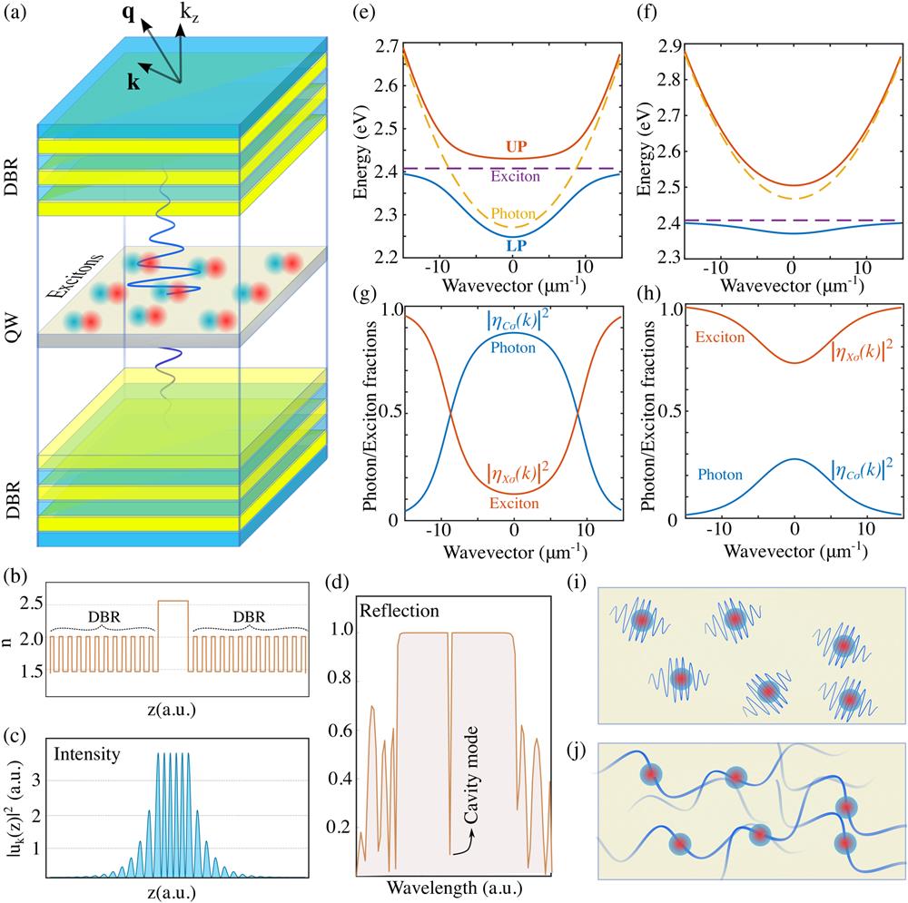
In semiconductor microcavities, exciton polaritons emerge from strong coupling between confined photons in cavities and excitons in semiconductors[41,42]. Typically, exciton polaritons are studied in the geometry shown in Fig. 1(a), where a semiconductor is sandwiched by two distributed Bragg reflector (DBR) mirrors to form an optical cavity, which is the so-called planar microcavity. While in free space light travels with a zero rest mass, in optical cavities, it acquires an effective mass due to confinement[43]. With perfect confinement along the axis, wave vector component in the same direction becomes quantized, such that only a discrete set of values ( for ) is allowed. Each quantized represents a photonic energy branch, within which the is fixed, but the in-plane wave vector component is a variable two-dimensional (2D) vector. The dynamics of microcavity photons in such a branch is given by an effective 2D description. For a strong confinement along the direction, the energy separation between quantized branches with different is large, and one can consider a single branch at once. In the following theoretical description, a single branch is considered for cavity photons, although generalization to the case of multiple branches is straightforward.
Figure 1.Fundamentals of microcavity exciton polaritons. (a) Schematic of a semiconductor microcavity, which consists of two distributed Bragg reflector (DBR) mirrors and a semiconductor quantum well (QW). The photons trapped inside the cavity formed by the DBR mirrors interact with the excitons (electron–hole pairs) in the QW. (b) Example of the schematic variation of refractive index n along the growth direction (z axis) of a microcavity. The periodic variation of low and high values of the refractive index forms a DBR. Two face-to-face periodic structures (DBRs) form a cavity where the QW (here with a higher refractive index) is embedded. (c) Intensity distribution |uk(z)|2 along the z axis of the photonic mode trapped inside the cavity. (d) Reflection from the microcavity, which shows a stop band (flat region where the reflection is almost one) and a cavity mode as indicated in the figure. (e), (f) Dispersion of upper (UP) and lower (LP) polariton modes (solid lines), which emerge from the strong coupling between photons (yellow dotted line) and excitons (purple dotted line) for different detunings between excitons and the cavity mode. (g), (h) Exciton (|Xσ(k)|2) and photon (|Cσ(k)|2) fractions of the lower polariton mode as functions of the wave vector for different detunings between excitons and the cavity mode. These fractions are given by the Hopfield coefficients Xσ(k) and Cσ(k). (i) Classical Bose gas with the average interparticle distance much larger than the thermal de Broglie wavelength (T). (j) Quantum gas (Bose–Einstein condensate) with the average interparticle distance comparable to T.
Microcavity exciton polaritons are fundamentally many-particle systems, where many photons and excitons interact with each other. In quantum theory, many-particle systems are described by quantum fields, which associate creation and annihilation operators to each point of space[44]. We will first consider the general properties of bosonic fields, and then consider the application of the formalism to photons and excitons. A bosonic quantum field represents an annihilation operator at position in a 2D plane and acts on the so-called Fock space with the spin projection on the axis. Similarly, represents a creation operator at position and spin projection . In quantum field theory, the bosonic field operators follow the canonical commutation relations (which play crucial roles in quantum statistics): where is the Dirac -function in two dimensions. The field operators can be written in reciprocal space as
Following the canonical Bose commutation relations shown in Eq. (1), we find that the creation and annihilation operators in reciprocal space [ and , respectively] satisfy the following commutation relations[44]:
These commutation relations are associated with the Bose statistics of quantum particles, which allows bosons to occupy a single quantum state in large numbers. This is fundamentally related to the polariton condensate that we will elaborate in Section 2.3.
2.1.1 Cavity photons
The confined cavity photons with the quantized wave vector (where is the quantization number) have a discrete set of energy branches: ɛ︀, where is the speed of light in free space, is the refractive index, and is the in-plane component of wave vector . Within a quantized branch, while is a constant, the 2D in-plane part is a continuous variable. Thus, the low-energy dispersion () is given by an effective 2D dispersion relation: ɛɛ︀where ︀, and ɛ is the mode energy at the zero in-plane wave vector. It is intriguing to note that while photons in free space show linear dispersion with zero rest mass, the photons confined in a cavity follow a parabolic dispersion relation with an effective mass .
In quantum theory, the microcavity photons are represented by a bosonic field with the spin polarization projection along the axis (growth axis of the microcavity), which is associated with the left and right circular polarizations of light. With a polarization-dependent effective mass , the cavity photons can be described by a Hamiltonian: ɛ︀
This is a common form of a Hamiltonian describing particles with a nonzero mass[45]. Using the reciprocal space representation of the field as given by Eq. (2), the photonic Hamiltonian can be rewritten in a simpler form: ɛwhere ɛɛ︀ is the quadratic dispersion relation of the cavity photons, which relates the energy with wave vector , and ɛ represents the constant energies at the zero in-plane wave vector, is the polarization projection on axis, and and are the reciprocal space annihilation and creation operators, respectively, corresponding to the photon field . For a physical interpretation, one can connect electric field of the cavity photons to the creation and annihilation operators[46]: where is the unit vector along the direction of polarization component , and is the profile of electric field along axis [see Fig. 1(c) for an exemplary profile along the direction].
While for simplicity the dispersion relation ɛ in Eq. (6) is considered diagonal for , in general, dispersion relations might have off-diagonal elements. Thus, a general form of the Hamiltonian for cavity photons is given by ɛ
Parameters ɛ represent elements of an energy matrix written in the basis of polarization projections () on the growth axis ( axis). While the diagonal elements represent the energy of a photon for a given polarization, the off-diagonal elements represent the coupling between different polarization modes. For instance, birefringence may cause a different effective mass along the crystal axis ( axis) and the perpendicular axis ( axis). Furthermore, the dispersion relations can be polarization dependent due to crystal anisotropy[47], such that the effective dispersion for the and polarization components is given by ɛɛ︀︀where ɛ is the energy at zero in-plane momentum, and and are the effective masses along two perpendicular axes and , respectively, for linear polarization component . While this dispersion ɛ is diagonal in the linear polarization basis, it is not diagonal in the circular polarization basis (). In the following description, we will use notations ɛ and ɛ for diagonal dispersions in circular () and linear () polarization bases, respectively.
2.1.2 Excitons
In semiconductor microcavities, thin layers of semiconductors are placed inside the cavities to realize strong interaction between light and matter. The low-energy optical excitation corresponds to the creation of electron–hole pairs (so-called excitons) in the semiconductor layer. Excitons emerge from the Coulomb interaction between electrons in the conduction band and the holes in the valence band. A sufficiently thin semiconductor layer acts as a 2D QW, where the electrons and holes are confined. Since electrons and holes are oppositely charged, they form bound states like hydrogen atoms in 2D with a characteristic length called the Bohr radius. Depending on the relative size of the Bohr radius with respect to the crystal lattice constant, excitons are typically classified as Frenkel excitons (with Bohr radii similar to lattice constants) and Wannier–Mott excitons (with Bohr radii extending several lattice constants). It is interesting to note that while the Bohr radius is inversely related to the exciton binding energy, it is directly related to the interaction between excitons[48,49]. Since the nonlinear interaction strength scales linearly with the exciton binding energy but quadratically with the Bohr radius, an intermediate value of the Bohr radius is thus preferable to obtain a sizable interaction strength as well as a decent binding energy.
To obtain room temperature polaritons, excitons must withstand corresponding thermal excitation energy , where is the Boltzmann constant, and is the temperature. This is possible for exciton binding energies . In this regime, low-energy physics (where the typical distance between excitons is much larger than the exciton Bohr radius) can be understood by considering excitons as bosonic quasiparticles (composite bosons)[50]. The corresponding Hamiltonian describing the excitons is given by ɛwhere ɛ is the energy, and and are the bosonic creation and annihilation operators, respectively, with in-plane wave vector and spin . The exciton energy ɛ weakly depends on the in-plane wave vector . In typical experiments, the exciton energy can be approximated as a constant ɛɛ. Furthermore, excitons are bosons with possible spin projection . However, here, we consider only optically active ones with [51].
2.1.3 Light–matter interaction
To obtain strong coupling with the cavity mode, typically QWs are placed at the antinodes of the optical field, and the energy of the cavity mode is placed near the exciton energy. The interaction between excitons and cavity photons can be described by an interaction Hamiltonian [20,41,52]: ︀where ︀ is the light–matter coupling strength (︀ corresponds to vacuum Rabi splitting). The strong coupling regime is achieved when ︀ is larger than the linewidth, such that the coherent exchange between photons and excitons becomes reversible. In this regime, exciton polaritons emerge as hybrid light–matter quasiparticles with an anticrossing in the dispersion as typical experimental signatures[21].
2.1.4 Exciton polaritons
The Hamiltonian describing a system of cavity photons, excitons, and their interaction is given by [20]. We find that the total Hamiltonian is quadratic in field operators. We can thus diagonalize the Hamiltonian with a linear transformation:
Operators and represent the annihilation operators of exciton polaritons, which are composites of excitons and photons. Prefactors and are known as Hopfield coefficients. Subscripts LP and UP represent the lower and upper polariton branches corresponding to the eigenvalues and , respectively, given by ɛɛ︀ɛɛ
In Figs. 1(e) and 1(f), we show the lower polariton (LP) and upper polariton (UP) energy branches as functions of the in-plane wave vector k for different bare exciton energies ɛ. While the bare cavity photon ɛ and exciton ɛ branches (dashed lines) can cross each other [Fig. 1(e)] at ɛɛ, the polariton branches show anticrossing with a minimum gap ︀, which is considered a hallmark of the strong coupling regime. Since the composite of two bosonic fields is also bosonic, the polariton field operators satisfy the Bose commutation relations shown by Eq. (1). The Bose commutation relations yield . Typical variations of Hopfield coefficients for different parameters are shown in Figs. 1(g) and 1(h). Hopfield coefficients represent the amount of excitonic and photonic content in the exciton polaritons. Notably, near the crossing points between the bare cavity photon energy and the exciton energy, the Hopfield coefficients are equal. In most experiments, the relevant phenomenon can be described only by the LP branch, such that the effective Hamiltonian is given by[42]
Henceforth, we will consider only the LP branch for our discussion. From an experimental point of view, there are some prominent methods used to show polariton dispersion in an energy-momentum diagram. For example, goniometer-like angle scanning, pinhole translation, and Fourier-space projection methods can be used[53]. However, the most commonly used method is Fourier-space spectroscopy, i.e., angle-resolved optical spectroscopy, where the angle information in the far-field projection is used to provide direct access to the energy-momentum dispersion of exciton polaritons. Typically, a system of lenses is used to perform the imaging of the back focus of a microscope objective (objective lens), which encodes information about the angle of emitted, reflected, or transmitted light from a sample [Fig. 2(a)]. The back focal plane of the objective lens, which shows a radial–symmetric intensity profile, is then collected and focused through the entrance slit of a spectrometer and finally onto the sensor of a 2D charge-coupled device (CCD). The center of the collected far-field circle represents 0°, while the edge represents the maximum collected angle, determined by the numerical aperture of the objective. The narrow slits at the entrance of the spectrometer serve as a spatial filter that selects only the signal with µ, or alternatively any other narrow slice of momentum space. The center of the ring µ is related to the ground state of the polaritonic dispersion. The signal is then dispersed by a grating inside the spectrometer and imaged onto the CCD. The energy-momentum dispersion relation is obtained from the CCD detector in which each pixel line includes spectral information for a corresponding angle (in-plane momentum). Furthermore, the spatial and temporal coherence properties of exciton polaritons are typically investigated by optical interferometry where the most common configuration is a Michelson interferometer [Fig. 2(b)]. For this purpose, the emission from the sample is, in general, studied in real space. For details, the real space emission from the microcavity is sent to a beam splitter that splits the signal into two new paths. Along one path, a mirror is used to reflect the signal back, while along the second path, a backreflector is in general preferred. In this way, the reflected signal from the second arm is flipped in a centrosymmetric way, thus allowing to study the coherence properties along different directions in space. To change the time delay between the two arms, thus obtaining information about the coherence time, the mirror is mounted on a motorized delay line. Two reflected signals are then combined onto the sensor of a CCD and generate an interference pattern whose amplitude and visibility are used to study the first-order spatial and temporal coherence properties of polaritons.
Figure 2.Commonly used experimental methods. (a) Schematic of the angle-resolved photoluminescence setup with Fourier image configuration[35]. (b) Top, schematic of the Michelson interferometer setup. Bottom, illustration of centro-symmetrically interfered images.
Polaritons interact with each other due to their excitonic components. In the mean field regime, the interaction between polaritons manifests as nonlinearity, which plays an important role for many practical applications of polaritons. Although the actual form of the interaction between polaritons is due to Coulomb interaction between electrons and holes, the low-energy physics in the LP branch can be well described by an effective Hamiltonian[49,54]: where are constants representing the interaction strength between different spin components, and is the real space annihilation operator for the LP field, given by
The form of the interaction Hamiltonian is known as the contact interaction. Here, two polaritons experience interaction only when they contact each other (same position). This local nature of the interaction motivates us to express the interaction Hamiltonian in real space. However, can be equivalently written in momentum space[54].
2.1.6 External potential
Exciton polaritons are excellent candidates for simulating various model Hamiltonians. For this, designing various types of potentials for in-plane motion is required. Several strategies are considered for implementing such potentials in semiconductor microcavities. For instance, external metallic meshes[55–57], optically induced high-energy excitons[58], and chemical etching techniques[59,60] are used for generating external potentials (see Schneider et al. for a review[8]). In the domain of room temperature exciton polaritons, one of the most used methods is to modulate the local thickness of the top DBR mirror using an etched layer of a polymer on top of the semiconductor QW[47]. This method proved to be effective in implementing a range of lattice structures. It has been shown that it can implement a strong lattice where the bandgap between the lowest-energy s-band and p-band is much larger than the linewidth of the LP mode. In such structures, the potential is induced by modulating the local thickness of the cavity, such that the cavity photons experience a change in the local energy along the in-plane motion. This can be represented by a potential function for the cavity mode. Since the polariton is partly light, the potential is also experienced by the polaritons through its photonic component. The effective potential for the LP branch is approximately given by where is the photonic fraction, which is a function of Rabi splitting and detuning between the cavity mode and exciton energy. Note that although Hopfield coefficient depends on the wave vector, it can be approximated as a constant for a small energy range. Thus, this approximation would be valid for a small potential variation. A more accurate analysis can be performed by introducing directly in . However, that would require a more complex Hopfield transformation to diagonalize the Hamiltonian, which can be done numerically. It is also possible to induce a potential using the excitonic component. For instance, local potential energy can be tuned by increasing the local exciton population using optical excitation. In this method, the effective potential is created using the strong repulsive interaction between excitons and polaritons.
2.1.7 Plasmonic cavity
Although the majority of exciton polariton studies are based on a planar microcavity structure, alternatively, plasmonic nanostructures can concentrate electromagnetic (EM) fields to deep sub-diffraction volumes () with high field enhancement, which serves as another type of cavity for exciton polariton studies. Hence, despite the high loss from the metallic part[61], and low -factor compared to microcavities, plasmonic nanostructures can still achieve high figures of merit () for strong coupling at room temperature[62]. Plasmonic cavities have been carefully designed to realize strong couplings for quantum dots (QDs), molecules, and 2D materials[63]. Plasmonic cavities can be realized in different forms. For example, individual metal particles, such as nanoprisms[64,65], nanorods[66–68], or nanocubes[69], that support localized surface plasmons can be the simplest plasmonic cavities. These kinds of plasmonic cavities are widely used because they are not only able to realize strong coupling with different materials, but are also a good platform to study the behaviors and characteristics of exciton polaritons as well as tunability[70]. Metal particle arrays that support plasmonic resonance are also utilized to achieve strong coupling[71,72].
Other widely used plasmonic cavities usually consist of paired plasmonic structures, such as bowties[73,74] or nanoparticle-on-mirror geometry[75]. When the gap between the paired metal nanoparticles is in sub-nanometer range, an ultra-low mode volume and ultra-strong field enhancement can be obtained, which is more likely to overcome the limit of high emitter scattering at room temperature to realize strong coupling[75–77]. These kinds of ultra-compact plasmonic cavities are widely used to study strong coupling with different materials[62,78]. Their ultra-compact and small mode volumes can not only improve the vacuum Rabi splitting but also further reduce the effective exciton number contributing to coupling down to the single-digit level[62], which is promising for quantum optics applications.
Despite the high metallic loss, high- plasmonic cavities were also achieved via several mechanisms[79], such as surface lattice resonance, multipolar resonance, plasmonic Fano resonance, and Tamm plasmon resonance, and strong coupling and exciton polaritons were also realized at room temperature[80,81]. Otherwise, by combining plasmonic nanostructures with conventional microcavities, the plasmon microcavity can be obtained to study ultra-strong coupling in plasmon-microcavity exciton polaritons[82]. Plasmonic cavities with their diverse structures and versatile properties will still play important roles for research of strong coupling and exciton polaritons at room temperature.
2.2 Mean-Field Theory
Although exciton polaritons are fundamentally quantum particles, in most experiments, they are well understood with mean-field theory. In this regime, quantum fluctuations are considered insignificant, such that a quantum field can be replaced with a wave function in the quantum theory discussed in the previous section. For simplicity, we consider that each spin component evolves independently, such that we can suppress the spin index from the wave function. After taking the mean-field approximation, intriguingly, the dynamical equation for the LP mode is given by the GP equation[83,84]︀︀where is the time derivative of the wave function, is the effective mass of low-energy polaritons in the LP branch, represents the external potential, and represents the Kerr-type nonlinearity originating from polariton–polariton interaction and neglecting a constant energy shift (in fact, the energy shift can be included in the external potential). Here, we have considered a parabolic dispersion with an effective mass . However, the actual LP dispersion is given by Eq. (13), which is non-parabolic in nature. For a more accurate description, one can replace the kinetic energy part ︀ in Eq. (18) by the exact dispersion (note that wave vector is replaced by operator , which has the position space representation ). Nonetheless, Eq. (18) well describes the most fundamental aspects of low-energy exciton polaritons. The same GP equation (with different parameters) describes an interacting atomic Bose–Einstein condensate (BEC)[85]. However, exciton polaritons are inherently driven-dissipative in nature, where exciton polaritons decay due to finite lifetimes and gain from external excitations. In this section, we discuss these aspects of exciton polaritons.
2.2.1 Dissipation
The DBR mirrors in the microcavity are not perfect, allowing photons to leave the system after a certain number of coherent oscillations. Similarly, excitons are quasiparticles with finite lifetimes. These effects can be incorporated as an effective lifetime for exciton polaritons , which can be represented by a loss term in the GP equation[86]︀︀where ︀ is the rate of decay in the system. Note that this theory is valid in the strong coupling regime, where the light–matter scattering rate () exceeds the decay rate. Since polaritons with a finite decay rate leave the system, it requires to inject new particles to get a nonzero population. Broadly, different schemes of injecting particles can be classified into categories of coherent and incoherent excitations.
2.2.2 Coherent excitation
Polaritons can be injected coherently by a near resonant laser, such that the injected particles can reach the polariton mode without losing the coherence of the applied field. Coherent excitations can be introduced into the driven-dissipative GP equation by a source term[41,52]: ︀︀where is a coupling function of the LP mode to the incident optical field . In a uniform planar cavity, the coupling function can be replaced with a constant value . However, to introduce the external potential , often the uniformity of the planar cavity is compromised. In this situation, a spatially dependent coupling function is necessary[47].
2.2.3 Incoherent excitation
Although there are different methods to implement incoherent excitation, theoretically, it can be described by an effective non-Hermitian potential . The equation of motion for polaritons under incoherent excitation is given by[86]︀︀
In addition, here, a generalized complex nonlinearity coefficient is introduced[87]. The imaginary part represents nonlinear loss, which activates an effective decay channel at high polariton density. This term is effectively responsible for saturation in the polariton intensity. The microscopic origin of such a term can be found in kinetic theories of the polariton condensates, which essentially indicates that saturations in polariton density arise due to saturations in high-energy exciton reservoirs[86,88]. As an alternative to Eq. (21), one can introduce incoherent excitation through a polariton reservoir with a local density : ︀︀where is a phenomenological coupling constant. The reservoir density can be described by an effective rate equation[86]: where and are the phenomenological excitation profile and decay rate, respectively.
One of the widely used methods of implementing incoherent excitation is to apply a far-off-resonant laser, such that the injected polaritons go through scattering processes with several scattering channels before reaching the low-energy polariton mode. While microscopic processes involved in different systems could be different, typically incoherent injections result in an accumulation in the so-called bottleneck region of LP dispersion (this effect can be described with a kinetic Monte Carlo approach[89]). Further relaxation to the lowest energy state can involve impurity scattering, phonon–polariton[90], polariton–polariton, and polariton–exciton channels. In the phonon–polariton channel, exciton polaritons lose energy through coupling with the lattice vibration. The polariton–polariton channel gets activated at a large polariton density when the incoherent excitation strength becomes large enough. In this process, a polariton can relax to a lower-energy state by colliding with another one, which scatters into a higher-energy state[42]. In the polariton–exciton channel, polaritons lose energy by scattering with excitons[91]. During these processes, polaritons lose their initial coherence of the applied laser field. Similarly, incoherent excitation can be induced by electrical injection. These methods of providing gain into the system allow to demonstrate strong evidence for spontaneous coherence building in polariton condensates.
Although quantum theory can provide a more accurate and general description of exciton polaritons, the mean-field approach is highly successful in describing the condensate regime, where a large polariton population together with weak interaction supresses quantum fluctuations. In the next few sections, we will use the mean-field theory to describe various phenomena, such as polariton condensation, superfluidity, and related effects.
2.3 Bose–Einstein Condensate
It is a fundamental nature of bosons that many of them can occupy a single quantum state. This basic principle was proposed by S. N. Bose for photons to derive Planck’s quantum radiation law purely from the statistical nature of quantum particles. Extending this theory for matter particles, Einstein predicted that a noninteracting Bose gas could undergo a phase transition at low temperatures, where a macroscopically large number of particles can spontaneously occupy the lowest energy state of a system in thermodynamic equilibrium. This phenomenon is known as Bose–Einstein condensation. According to Bose statistics, the particle number distribution as a function of energy ɛ is given by ɛɛwhere is the Boltzmann constant, is the chemical potential, and is the temperature. A BEC essentially emerges from the fact that the average occupation number ɛ can diverge for ɛ. This phenomenon was observed with magneto-optically trapped atoms[92] at extremely low temperatures (e.g., 170 nK[93]).
In an ideal Bose gas, BEC occurs when the so-called thermal de Broglie wavelength ︀ exceeds the average interparticle distance [see Figs. 1(i) and 1(j)], where is the mass of the boson. Importantly, is inversely related to the effective mass . Thus, the critical temperature required to obtain a BEC is larger for a smaller effective mass . The effective mass of exciton polaritons is many orders of magnitude smaller than a typical atomic mass. In fact, the effective mass of exciton polaritons is only to times the mass of an electron . Thus, at a certain temperature , the thermal de Broglie wavelength of exciton polaritons is huge compared to the same for an atomic gas. For this reason, while a cryogenic temperature is required for an atomic BEC, it was long expected that exciton polaritons can exhibit BEC even at room temperature. However, polariton BEC can have certain differences compared to the traditional BEC. We will discuss more on polariton BEC shortly.
2.3.1 Global phase coherence
In quantum theory, a particle is described by a wave function . The same particle can be equivalently described by , where is a global phase (which is a constant for the whole space). This arbitrariness of the global phase is due to so-called gauge symmetry. In a gauge symmetric system, each particle is independently associated with an arbitrary global phase . Remarkably, all particles in a BEC can be described by a single wave function . Here, there is only a single global phase associated with the whole condensate rather than each particle having an independent one. Furthermore, since represents a macroscopic number of particles, the global phase of a condensate can be determined from interference experiments[94]. This technique was used in exciton polariton systems to show long-range coherence[28].
2.3.2 Exciton polariton BEC
Exciton polaritons are bosons and thus can condense into the lowest-energy state in the LP branch[95]. Although microcavity exciton polaritons are confined in 2D semiconductor planes and thus do not exhibit a strict BEC (Hohenberg–Mermin–Wagener theorem), local condensates with finite size can occur in 2D, where macroscopically large occupations and long-range coherence can be observed[4]. Moreover, the driven-dissipative nature allows to induce various kinds of condensate properties, which do not spontaneously arise in traditional bosonic systems. For instance, polariton BEC can be obtained with nonzero in-plane wave vectors or stable quantized vortices. In a driven-dissipative system, BEC occurs in a quantum state with the largest gain. The control on excitation profiles allows to induce maximum gain in a chosen spatial profile of the polariton BEC. In most experimental systems, polaritons have lifetimes shorter than energy relaxation time, which does not permit thermal equilibrium. Thus, polariton BECs might not follow the exact equilibrium Bose distribution. However, polaritons with longer lifetimes can show equilibrium BEC in high-quality microcavities[96]. Since polaritons escape the system due to finite lifetimes, they are widely studied in the steady state condition where the rate of loss is compensated for with an equal amount of external injection through coherent and incoherent excitations. The experimental signatures of the room temperature polariton BEC are discussed in Section 3. A polariton BEC is described by the driven-dissipative GP equation given by Eq. (18). Under incoherent excitation, the steady state solution can be obtained from the equation ︀
For simplicity, considering a uniform incoherent excitation , below the threshold , the only steady state solution is given by . However, above the threshold , one obtains nonzero solutions for the condensate wave function, where is an arbitrary global phase. This suggests that below the excitation threshold, polariton BECs cannot occur due to excessive loss. Above threshold, the system spontaneously chooses a solution with a particular value of the global phase (note that the global phase can be time dependent).
Under coherent excitation , the steady state solution can be found from Eq. (20). For simplicity, we consider a uniform planar cavity with a constant coupling function and define an effective coherent excitation amplitude . The steady state solution can be obtained with an ansatz , where satisfies ɛ︀where ɛ is the polariton energy at excitation wave vector . Note that the polariton density is simply given by , and the coherently applied excitation intensity is . The polariton density as a function of applied intensity can be obtained from Eq. (26). In general, there are three solutions for for a value of . However, for the parameter regime ︀ɛ, there is only one physical solution. In the regime ︀ɛ, can have two stable physical solutions for the same value of . These solutions represent the so-called bistable behavior of exciton polariton condensates[97,98]. The region of bistability is bound by two turning points in polariton density: ︀ɛ︀ɛ
These turning points can be obtained from the condition . Bistability is a signature of nonlinear behavior of polariton condensates, where the polariton density abruptly jumps to a higher value from a lower one for a relatively small change in excitation intensity. Bistability is a feature of a single nonlinear polariton mode, but the same nonlinearity can also induce intriguing effects when multiple modes are coupled, such as parametric scattering[99] and oscillation[100].
2.4 Superfluidity
Superfluidity is a state in which matter behaves as a fluid without viscosity. It is typically associated with several phenomena, such as the fountain effect, flow without dissipation, frictionless motion of impurities, and Hess–Fairbank effect. Superfluidity was first observed in liquid helium-4 at very low temperatures (below the so-called -point). The microscopic origin of superfluidity is closely related to the mechanism of BEC. In BEC, many particles occupy a single quantum state with a global phase coherence. In superfluidity, such a phase coherence allows a dissipation-less flow of mass in a fluid. In this direction, several experiments reported observations of superfluid signatures in exciton polariton systems, and most of them were in the domain of cryogenic temperature. Experimental signatures of exciton polaritons are discussed in Section 3.2.
A phenomenological criterion for superfluidity was developed by Landau[42]. It sets a critical velocity below which a weak impurity can travel without friction through the superfluid. The critical velocity is given by ɛ︀, where ɛ is the dispersion of the elementary excitations in the superfluid. The dissipation-less flow of a fluid is possible if the speed of the fluid is smaller than , where it is thermodynamically unfavorable to create excitations. A microscopic description of this theory was given by Bogoliubov considering a weakly interacting BEC[42]. This theory quantitatively recovers the excitation spectrum proposed by Landau. Here, a condensate with density of particles is perturbed by interaction to induce a normal component of the fluid through quasiparticle excitations known as Bogolons. The dispersion of these elementary excitations is given by ɛɛɛwhere ɛ︀, is the mass of a particle, and is the interaction strength at wave vector . Indeed, this spectrum shows a characteristic linear behavior in the small wave vector regime for a nonzero superfluid density . For a normal fluid, the superfluid density is zero, and one recovers the quadratic dispersion ɛɛ.
2.4.1 Quantized vortices
A fluid can form a vortex due to flow of mass with a finite rotational velocity around an axis. A superfluid with a uniform global phase does not allow such a rotational flow of mass. However, a sufficiently large perturbation can change the scenario with a spatially inhomogeneous phase . The wave function can then be written as where is the particle density. Mass flow in a fluid is described by a velocity field ︀. From the condition of single-valuedness of the wave function , one can show that the phase gradient satisfies the relation where is a closed loop, dl is the infinitesimal line segment on the loop C, and is an integer. The situation represents a homogeneous or weakly perturbed condensate. A nonzero value of represents a topological phase winding and thus a mass flow (since is related to ) around loop . This winding of the phase around a loop is known as the quantized vortex with an integer value of the winding number . Such topological vortices with quantized winding numbers are observed in exciton polariton condensates[7]. Their origin in time-resolved single-shot experiments has been described as scattering of the coherent polariton condensate with a fixed disorder potential[101].
Let us consider that the phase of a vortex is given by , where is the angle in polar coordinates. Here, the phase winds times around the point . Considering loop as a circle with radius , one finds ︀where is the unit vector along the angular direction. As can be seen, the angular velocity increases rapidly as particles approach the center (the vortex core); to support a vortex with finite energy, the superfluid density must vanish at the center.
2.4.2 Berezinskii–Kosterlitz–Thouless transition
In a 2D Bose liquid, vortices are the elementary topological excitations, which may appear with positive and negative winding numbers. Excitations with positive and negative winding numbers are known as vortices and antivortices, respectively. At a finite temperature, vortex–antivortex pairs can be spontaneously unpaired by thermal excitations. In a thermodynamically large system, there is a characteristic temperature above which the thermal energy is sufficient to activate enough numbers of freely moving vortices and antivortices to destroy the global superfluidity. Below , the thermal energy is insufficient to unpair the tightly bound vortex–antivortex pairs, and thus, they can only weakly perturb the local superfluidity. Thus, if the temperature is tuned around , the system goes from a normal fluid to superfluid phase transition. This is known as the Berezinskii–Kosterlitz–Thouless transition[102,103].
2.5 Quantum Regime
The quantum fluids of light emerge from the microscopic quantum mechanical behavior of exciton polaritons. However, as we have seen, they are well represented by the driven-dissipative GP equation, where quantum fluctuations play no significant role, such that mean-field theory is enough to describe the system. In the fully quantum regime, many-body quantum interactions between polaritons take the central role. In this regime, polariton–polariton interaction cannot be approximated as mean-field nonlinearity with the approximation . Here, one must consider the full quantum interaction Hamiltonian given by Eq. (15). Within this regime, one can further distinguish between the collective quantum effects and quantum effects in an individual polariton mode.
2.5.1 Collective quantum effects
In this regime, systems of many coupled quantum modes are considered. While each quantum mode may appear simple to understand, all modes together can represent a complex interacting many-body quantum system. Here, collective phenomena such as phase transition, critical effects, and long-range correlations are studied. A system of driven coupled quantum modes can be described by the Hamiltonian : ɛwhere ɛ is the energy, is the coupling energy, is the interaction strength, and is the coherent excitation amplitude. The dissipation of quantum modes can be incorporated by a quantum master equation: ︀︀where is the density matrix, and ︀ is the decay rate. As can be seen, the system is characterized by global parameters ɛ, , , and . Here, one might not control the individual quantum modes. This regime is relevant to the so-called quantum simulators, where one aims to understand idealized quantum systems (which may not occur in nature) using polaritons as a controllable many-body system.
2.5.2 Single-mode quantum effects
So far, we have presented polariton systems with many coupled quantum modes, each of which is associated with a real (e.g., ) or reciprocal [e.g., ] space index. This is indeed suitable for simulating collective many-body physics. However, there is another quantum regime where one controls the polariton modes individually. This regime is relevant to the rapidly emerging quantum technologies[104–106], such as quantum computing and quantum information processing. Here, an isolated single quantum mode is considered and manipulated individually. An isolated quantum mode can be associated with an annihilation (creation) operator () and can be described by a Hamiltonian given by ɛwhere ɛ is the energy difference between applied laser energy and mode energy, is the quantum interaction coefficient, and is the applied laser amplitude. The radiative loss can be incorporated by a Lindblad term in the quantum master equation. Note that even a single quantum mode can be occupied by many polaritons due to their bosonic nature. However, strong quantum interaction between polaritons can prevent multi-particle occupation due to a strong interaction-induced blue detuning. This is the so-called polariton blockade effect[107]. However, for this effect to be efficient, one needs to resolve the blue detuning in the energy spectrum, where there is a natural energy broadening due to the finite linewidth . An efficient polariton blockade is thus possible for . Achieving this regime is in principle possible in strongly localized polariton modes in micropillar-like geometries, where the polariton–polariton interaction can be greatly enhanced. The polariton blockade is quantified with a second-order correlation function:
For a strong polariton blockade, , and noninteracting modes with show the absence of blockades. An alternative mechanism to achieve a polariton blockade is the so-called unconventional blockade, which utilizes an interference induced effect[108–110]. An unconventional blockade occurs even in weakly interacting polaritons, which are more accessible in the current experimental conditions. However, in an unconventional blockade, the correlation function shows rapid oscillations as a function of , which makes it hard to observe for polaritons. More recently, dynamical mechanisms have been proposed, where a polariton blockade is induced by a time-dependent parameter in the Hamiltonian[111,112]. For instance, a combination of pulsed and continuous wave excitation can be used to induce periodic (in time ) windows of a strong blockade. In this dynamical blockade, there is no rapid oscillation in , and thus, it is suitable for observation in polariton systems. Another advantage of a dynamical blockade is that it can operate in regimes of both weak and strong interactions[111].
Beyond the blockade effect, a strongly interacting single-mode polariton condensate can be used as an elementary quantum bit (qubit) for quantum computation[113]. A qubit is a two-level quantum system, where a single quantum of excitation is controlled and manipulated. Although a condensate itself can be occupied by a large number of polaritons, strong interaction can induce significant quantum fluctuation. Quantum fluctuation on top of a single-mode condensate can be described by considering the number operator , where is the average number of polaritons in the condensate, and is the number fluctuation on top of the condensate. Using the Hamiltonian , one can show that the fluctuation is described by an effective Hamiltonian [113]: where is the phase operator satisfying , the complex parameter is the applied laser amplitude, and is the effective detuning. Due to the cosine term, this Hamiltonian represents an anharmonic oscillator, which has a nonuniform energy spectrum. This means that the energy gap between the ground state (with energy ) and the first excited state (with energy ) can be much different from the energy gap between the first and second excited states and other higher energy gaps. Due to this nonuniformity in the energy spectrum of , the low energy excitation dynamics can be restricted into the subspace formed by the two quantum levels and . However, the energy gap must be larger than the linewidth to achieve a long-lifetime qubit.
2.6 Applications
Exciton polaritons are attractive systems to realize a wide range of phenomena related to condensed matter physics and optics, both of which have provided plenty practical applications. It is then naturally motivating to find applications for exciton polaritons. Over the past decades, the richness and maturity of the field of exciton polaritons have allowed to find several proposals for applications. However, their experimental prototypes work mostly in the regime of cryogenic or low temperatures. From the application side, room temperature operation of a device is essential for cost effectiveness. Thus, the recent success of room temperature exciton polaritons has motivated the polariton community to revive some of the earlier proposals and further review new ideas for applications.
2.6.1 Polariton laser
Bose–Einstein condensation is a natural source of a large population in a single energy mode with phase coherence, which can be used for the same function as lasers do for photons. Indeed, atomic BEC was proposed as a laser providing coherent atoms[114,115]. In this context, polaritons in semiconductor microcavities are attractive. They are hybrid particles combining characteristics of matter and light. While polaritons can condense into a single energy state with a large population like an atomic BEC, they can also emit photons retaining the phase coherence and monochromaticity of the condensate. Polariton lasing was thus envisioned with intriguing characteristics and closely related to BEC[116]. An attractive feature of polariton lasers is that they can operate with significantly lower thresholds compared to their photonic counterparts[35,117–120].
Even though the output actions of both types of lasers are the same, the underlying mechanism of polariton lasing is very different from that of standard photon lasers[11]. In a photon laser, phase coherence is established by stimulated emission in a system with a massive number of photons with the help of so-called electron population inversion. Note that photon and polariton lasing can both occur in the same system, but in different regimes of parameters. In semiconductor microcavities, photon lasing may occur in the so-called Mott density limit, where the exciton binding energy diminishes because of Coulomb screening and the interaction between excitons. In this limit, electron–hole pairs cannot be approximated as bosonic quasiparticles. Here, the formation of an electron–hole plasma, the stimulated photon emission into the cavity mode, and electron population inversion are all allowed. With these conditions fulfilled, photon laser action begins[121].
In polariton lasers, electron population inversion is not required. Here, the coherence originates from the formation of BECs [see Fig. 3(a) as reported by Kasprzak et al.[122]], which occurs at an exciton density much lower than the Mott density. Since excitons are injected via external excitation, achieving the Mott limit for photon lasing would require more energy than reaching the BEC regime (a lower threshold). In this regime, the bosonic nature of excitons is conserved, and strong coupling between excitons and cavity photons allows the formation of polaritons. These composite quasiparticles then can obey Bose statistics, which is at the heart of polariton lasing[116]. Here, injected high-energy polaritons go through several scattering processes (e.g., polariton–polariton, polariton–exciton, and polariton–phonon scatterings) and relax to a low-energy state in the LP branch where it forms a polariton BEC. The photon emission from the polariton BEC due to decay (finite lifetime) then acts as lasing action.
Figure 3.Applications of microcavity exciton polaritons. (a) Angle resolved photoluminescence below threshold (left), at threshold (middle), and above threshold (right). The polariton condensate above threshold acts as a polariton laser[122]. (b) Lattice simulator for realizing topological insulator using exciton polaritons under a strong magnetic field[134]. (c) Left: schematic of a room temperature lattice simulator using intrinsic anisotropy of perovskite microcavities. Right: eigenvalues in trivial (W = 0) and topological (W = 1) phases of the simulated Su–Schrieffer–Heeger model[135]. (d) Top: scheme of an all-optical polariton transistor. Bottom: real space emission image of address beams A and B and control beam C[14]. (e) Top: schematic representation of a polariton neuromorphic computer for handwritten digit recognition. Bottom: experimental scheme of modulating a laser beam with spatial light modulator (SLM) and a CCD camera to get the output[161]. (f) Left: proposal for realizing qubits using quantum fluctuations in polariton condensates. Right: fidelities of polariton quantum gates (SWAP and sSWAP) as functions of lifetime compared to the interaction strength[168].
BEC represents a macroscopic number of particles in the ground state of a system. It is thus suitable for simulating materials at low temperatures, where the ground state properties are the dominating features. Typically, the Hamiltonians representing materials are complex, and thus exact analyses of them are difficult. While approximate theories can be used to understand many important features, they are not reliable in all parameter regimes. This problem can be solved by simulating Hamiltonians using BEC in tunable physical systems. While tunability provides the reach to different parameter regimes, BEC provides accurate ground state features. Note that measurements on macroscopic numbers of particles provide accurate results with small statistical errors.
Typically, BEC is used to simulate lattice systems, which describe various condensed matter systems. In cold atomic systems, counterpropagating lasers are used to design optical lattices[123]. Polariton BEC is also suitable for simulating intriguing lattice systems[124], e.g., topological[125–127], nonreciprocal[128,129], flatband[130,131], and honeycomb lattices[132,133]. For instance, see Fig. 3(b) for a scheme of a simulated topological insulator using an exciton polariton lattice as was shown by Klembt et al.[134]. One of the major advantages of polariton BEC is that it can operate at room temperature, which is much easier to achieve than reaching an extreme cryogenic temperature for atomic BEC lattices. For this reason, polariton simulators are scalable and readily implementable for room temperature operations [see Fig. 3(c), which is adopted from Su et al.[135]]. Moreover, exotic features of materials such as halide perovskites and TMDs provide additional controls on the lattice design.
In polariton BEC, lattices can be implemented by using periodic external potentials. A single site in a lattice is created by a local potential well , which is centered around position . For instance, the potential well can be a circular region around point such that , where is the depth of the potential, and is the radius of the circular region ( is the Heaviside step function). This isolated site represented by is a finite 2D potential box, which can have many bound eigenstates for a sufficiently large value of . Let us consider that these bound eigenstates are with eigenvalues , such that , where , and is the kinetic energy part of the Hamiltonian. A lattice can be generated by introducing many such sites with , such that the total Hamiltonian is given by . The low-energy subspace of the total Hamiltonian can then be spanned by eigenvectors : where coupling energies between sites and are given by . This represents a lattice Hamiltonian, when the coupling energy is much smaller than the energy gap between the lowest-energy state and the first excited state within a site, i.e., for any and . Here, are called onsite energies, and are called hopping amplitudes between sites and . Typically, the hopping amplitudes can be controlled by geometrical proximities between corresponding sites. A large distance between sites would induce small hopping amplitudes, and one can consider significant hopping only between the nearest neighbor lattice sites. Introducing additional channels between the lattice sites can further enhance the nearest neighbor hopping amplitudes[47]. However, with appropriate geometries, one can induce significant hopping beyond the nearest neighbor sites.
Lattice design can be greatly enhanced with extra features such as anisotropy and birefringence in perovskite microcavities. Here, the effective masses of polaritons along and axes are different and polarization dependent. Depending on the linear polarization projections ( and ) and crystal axes ( and ), the effective LP mass can take four different values , where the directional index , and the linear polarization index . Thus, for a given polarization projection , one obtains different hopping amplitudes by aligning the lattice sites in different directions. For instance, if two sites and are aligned along the axis, ︀which can be further generalized for arbitrary alignment. These directional and polarization dependences of hopping amplitudes provide additional freedom to fabricate exotic lattice simulators.
Another element in lattice simulation is the so-called artificial gauge fields[136]. Exciton polaritons are electrically neutral particles, and thus, they do not couple to the EM field in the same way as charged particles do. However, exciton polaritons do respond to the applied EM field due to their nonzero dipole moment. Using this effect, one can induce artificially created gauge fields for polaritons to simulate charged particles in an actual EM field[137]. Such artificial gauge fields can be used to simulate various physical effects in polariton systems, e.g., quantum Hall effect, topologically protected propagation, and Hofstadter’s butterfly[126,138]. Furthermore, other exotic effects can be simulated by utilizing polariton nonlinearity[44,139,140].
2.6.3 Optical computing
Optical computing uses light for propagation and processing information[141]. Optical computers promise ultra-low power consumption, high processing speed, and extremely low losses. However, realizing an all-optical computer is a complex task. Present-day computers process data in the form of binary digits, which can have a value of zero or one. It is then processed with operations made with elementary gates, such as AND, OR, and NOT gates. One of the major challenges in the domain of optical computing is to find strong nonlinearity, such that these elementary gates can be implemented simultaneously in the same system. Exciton polaritons with strong nonlinear properties can be an excellent platform for optical computing. However, if these computers must compete with electronic computers, their room temperature operation is necessary. In this direction, an exciton-polariton-based optical transistor was shown to operate at room temperature[15], and previously at lower temperatures as shown by Fig. 3(d)[14]. In fact, transistors are used in digital computing as electronic binary switches, which can be put into “on” and “off” states by controlling flows of electrical currents with gate voltages. An optical version of this binary switch can be obtained, where propagation of an exciton polariton condensate can be controlled by optical fields. Recently, room temperature operation of an all-optical binary switch was indeed demonstrated using self-assembled perovskite microwires[142]. Other required optical components such as memory devices[143,144], diodes[145,146], routers[147–149], and optical amplifiers[150] are required for room temperature optical computing. A universal logic gate set and a method of cascading them are also required[151].
Another promising computing architecture is the optical spin simulator. Here, certain computational tasks are transformed to problems of finding the ground states of spin models. For instance, spin simulators were shown to find the global ground state configuration using interconnected graphs of local exciton polariton condensates[152]. In this method, the global minimum of the Hamiltonian is reached by the so-called bottom-up approach, such that the system naturally condensates at the minimum energy state[153]. This approach is very different from commonly used methods in classical and quantum annealers. Similarly, the classical Ising model can be realized with exciton polariton condensates, which can be used for global optimization of non-deterministic polynomial-time-hard (NP-hard) problems[154,155]. Alternatively cellular automata based on exciton polaritons can be used for computing[156].
2.6.4 Neuromorphic computing
Artificial neural networks (ANNs) are information processing systems inspired by biological brains. ANNs are collections of interconnected nonlinear nodes that mimic biological neurons, and their connections are like synapses in brains. Typically, neurons are arranged in layers, where the connections can be allowed within and between layers. Information travels from the first (input) layer to the last (output) layer, possibly after going through multiple (hidden) layers in between. ANNs can be implemented as software in digital computers based on the so-called von Neumann architecture, where the processing unit is physically separated from the memory unit. The communication between these two physical units causes a time delay, which puts a limit on computing speed no matter how fast a given processor can work. This is known as the von Neumann bottleneck, which is considered as a problem that can be overcome only by changing the computing architecture. Since ANNs do not require physical separations between memory and processors, they can be physically implemented as independent computers. The physically implemented ANNs are known as neuromorphic computers, which benefit from native parallelization and are free of the von Neumann bottleneck. Among various possibilities, exciton polaritons can be excellent platforms for neuromorphic computing due to their unprecedented photonic nonlinearity. However, ANN works on the principle of learning, where network connections are slowly adopted to a set of parameters such that it can produce a desired output. For this, individual connections between nodes must be controlled precisely[157,158]. This is a challenging task for networks with massive numbers of nodes. This problem was solved using a relatively lesser-known neural network architecture called reservoir computing[159]. In reservoir computers, the main physical part of the neural network is kept fixed with a random set of connections and only a single layer of output connections is controlled[160]. Here, the random network can be formed with polariton BECs in lattices with random hopping amplitudes [see, for instance, Fig. 3(e) where a polariton neural network is used for classifying handwritten digits][161,162]. The output layer is controlled externally after a readout in the form of photoluminescence from the polariton lattice. It was also shown that the driven-dissipative nature of exciton polaritons can be taken as an advantage for better performance[159], and that that small-scale polariton reservoir computers can be used as building blocks for digital computing with natural robustness to noise and error[163]. So far, these networks work in the domain of cryogenic temperature. The recent advancement in room temperature exciton polaritons inspires the possibility of polariton neural networks working in ambient conditions.
2.6.5 Quantum simulation
Quantum simulators are devices that use quantum effects (e.g., entanglement and superposition) to understand physical systems through studying model systems[125,164]. They can be used for a wide range of applications, including drug design and material manufacturing. It was suggested by Feynman that quantum devices would be better for modeling certain systems that cannot be efficiently done by classical devices[165]. For instance, typically quantum systems are simulated using numerical tools such as mean-field theory, dynamical mean-field theory, density functional theory, and Monte Carlo algorithms. All of them have their limitations and cannot be applied for all systems in all regimes. Some can be used as complementary methods in different regimes of parameters. However, there are many examples where no numerical method can escape the slowdown in computational time due to an exponential rise of the Hilbert space dimension with respect to the number of particles. A typical example of such a system is a quantum spin model with arbitrary couplings between spins. For this reason, quantum devices are considered crucial for modeling quantum systems in large scale.
Exciton polaritons can be used as a platform to implement quantum simulators. In the strongly interacting regime, where interaction between exciton polaritons exceeds the linewidth, quantum correlations between different particles become important. In this regime, exciton polaritons can show quantum effects beyond mean-field condensate behavior. These effects can be used for quantum simulations. For instance, let us consider a Bose–Hubbard model, which is a prototypical system to study a Mott insulator to superfluid transition. The corresponding Hamiltonian is given by
Depending on the ratio between and , one can get a superfluid phase with or Mott insulator phase with . This Hamiltonian can be obtained in an exciton polariton lattice with strong polariton–polariton interaction. Similarly, the Jaynes–Cumming model[166] and quantum spin models[167] can be implemented, in principle, in semiconductor microcavities. Here, the driven-dissipative nature could be a limitation for simulating strictly equilibrium properties. However, driven-dissipative versions of these quantum models are equally interesting and can be used for simulating open quantum systems.
2.6.6 Quantum computing
We have seen that an effective two-level system can be obtained using a strongly interacting single-mode polariton condensate. This two-level system can contain at most one quantum of excitation provided by an applied laser as schematically shown in Fig. 3(f), which is adopted from Ghosh et al.[168]. Thus, this system can indeed serve as an elementary quantum bit or qubit for quantum computation. Let us now discuss how this system can be effectively controlled by the applied laser field. From Eq. (36), we find that the low-energy Hamiltonian describing the qubit is given by where ︀ is a 3D energy vector, is a vector consisting of Pauli matrices, and is the laser detuning (a similar qubit Hamiltonian was obtained in Ref. [169] using a polariton vortex). This is the most general form of a Hamiltonian, which can be fully controlled by , and (all are laser parameters). There are several advantages of polariton qubits: precise qubit control is possible by tuning the frequency, amplitude, and phase of the laser;operation can be fast with a time scale of few picoseconds;the system is scalable to many qubits;operation temperature can be as high as room temperature.
Even though finding a suitable system for a qubit is a significant step, suitable quantum gates must be designed to obtain a functional quantum computer. It is shown that any quantum operation can be approximated as a combination of single- and two-qubit quantum gates. Furthermore, these gates can be chosen from a small set of universal gates. For instance, single-qubit gates and controlled-NOT (cNOT) are a universal gate set. Similarly, the square root of a SWAP (sSWAP) gate and single-qubit gates are also a universal gate set.
As can be seen in Eq. (40), the single-qubit Hamiltonian is fully tunable by laser parameters. Thus, by sending a laser pulse, one can induce arbitrary unitary gate ︀, where is the pulse duration, and the pulse is a constant for a time window . Achieving two-qubit quantum gates is more subtle[113]. Here, two qubits need to interact for a brief time to induce a gate. Indeed, polaritons in two different condensates can interact. For instance, polariton condensates can be achieved in the two different polarization components, and they can interact via the Hamiltonian given by Eq. (15). This interaction Hamiltonian in qubit space can induce a cNOT gate. Furthermore, polariton condensates can be coupled simply by placing them close to each other. If the distance is small enough, quantum tunneling of polaritons induces the so-called Josephson coupling between condensates. Such a coupling can induce sSWAP and SWAP gates between two qubits. Note that the Josephson coupling or the interaction between couplings can be effectively switched off by introducing a large energy detuning between qubits. Similarly, quantum gates can be realized using polariton propagation in nonlinear waveguides, where polariton interaction plays a central role[170]. There are also schemes of quantum computing based on continuous variable states[171,172].
3 Development of Room Temperature Exciton Polaritons
In the previous section, we presented an introduction to exciton polaritons in semiconductor microcavities and related physical phenomena. We also reviewed the possible applications of exciton polaritons. In this section, we present an in-depth review of the recent achievements of room temperature exciton polaritons in various physical systems.
Experimentally, the history of microcavity exciton polaritons dates back to earlier GaAs and CdTe systems. However, limited by their small exciton binding energies, such systems can work only at cryogenic temperatures, where their exciton, and thus exciton polariton, can stably exist. In the room temperature polariton framework, one of the prerequisites is that a system should possess large exciton binding energy against room temperature thermal fluctuation (26 meV), where excitons must be stable at room temperature. When semiconductor excitons are coupled to cavity photons, in general, there will be two main regimes, weak and strong coupling regimes, which are determined by the interplay of coupling between particles and their dissipations. If the relation between coupling strength (︀; ︀ corresponds to the vacuum Rabi splitting energy) and dissipations ( for cavity photons; for excitons) satisfies ︀, the system reaches into the strong coupling regime. Otherwise, a weak coupling regime is achieved[3]. In this sense, one could either enhance the coupling between excitons and cavity photons or reduce their dissipations by improving their lifetimes to reach the strong coupling regime at room temperature.
In the past few decades, various kinds of semiconductor systems have emerged as promising candidates for exciton polaritons in the strong coupling regime at room temperature, such as ZnO[29,30], GaN[31], OSCs[32–34], halide perovskites[3,35,36], monolayer TMDs[37], and carbon nanotubes[38–40]. Although these systems work in different energy ranges, their major similarities are that they typically have strong exciton binding energies and high exciton oscillator strength, which allow to conveniently satisfy the criteria of the strong coupling regime, and they have achieved rapid progress in recent years, as shown in Table 1. In the following, we will introduce these systems roughly following a historical timeline.
Material Type
Exciton
Material
Morphology
Synthesis
at 300 K (eV)
(meV)
Rabi Splitting (meV)
Ref.
Traditional inorganic
Wannier–Mott
GaN
Bulk
MBE
3.42
25
31–60
[31]
QW
MOVPE
3–3.3
40
17–56
[173]
Microwire
MOVPE
3.42
25
115
[174]
Wannier–Mott
ZnO
Microwire
Carbothermal method
3.31
60
200–330
[29]
Bulk
PLD
3.31
60
50–260
[30]
Traditional organic
Frenkel
J-aggregates
Film
Solution method
1.8
360
80-160
[32]
Anthracene
Single crystal
Melt-grown method
3.16
640
86–256
[33]
TDAF
Film
Thermal evaporation
3.5
NA
600–1000
[175]
Conjugated polymer
Film
Spin-coating
2.7
116
[176]
Halide perovskites
Wannier–Mott
(, Br, Cl)
Film/flake
Spin-coating/exfoliation
2.3–3.14
200
90–230
[177–184]
Film
Spin-coating
2.3
30
70
[185]
Nanowire
Solution method
2.3
390
[186]
Nanoplatelet
CVD
2.407
40
120
[36,47,99,100,187]
Nanowire
Solution method
2.407
200
[142,188]
Nanoplatelet
CVD
3.04
70
270
[35,189]
()
Crystal
Exfoliation
1.56–2.55
125–470
NA
[190,191]
Transition metal dichalcogenides
Wannier–Mott
(, W;, Se)
Flake
Exfoliation/CVD
1–2
320–720
11.4–780
[37,120,192–196]
Carbon nanotubes
Wannier–Mott
Single-walled carbon nanotubes (SWCNTs)
SWCNTs in thin polymer film
Solution method
0–2
300–500
35–127
[38–40,197,198]
Table 1. Comparison of Room Temperature Polariton Semiconductor Systems.
Early studies on exciton polaritons working at room temperature date back to wide-bandgap inorganic semiconductors, such as GaN and ZnO, which typically show the advantages of a non-toxic nature and high stability. They typically operate in the UV regime where GaN in wurtzite crystal structure is a III/V direct bandgap semiconductor with a large bandgap of , and ZnO in wurtzite crystal structure is a II/VI direct bandgap semiconductor with a large bandgap of 3.3 eV. As well-established semiconductor systems, they are well known for excellent exciton properties, such as strong exciton oscillator strength and large exciton binding energies of 25 meV for GaN and 60 meV for ZnO, satisfying the basic criteria for strong coupling at room temperature. As a result, they allow robust exciton polaritons at room temperature, providing new platforms for investigating polariton lasing (including electrically injected), and intriguing nonlinear effects. Typically, a cavity quality factor is crucial to reduce dissipations for realizing the strong coupling regime. This was challenging for III-N-based heterostructures to grow crack-free and highly reflective nitride DBRs with GaN and (Al,Ga)N layers[199,200], which is usually caused by a large mismatch between the lattice constants of GaN and AlN (2.7%) and a difference in their thermal expansion coefficients of and for GaN and AlN, respectively. To overcome this challenge, different geometries were explored such as GaN microcavities based on bulk, membrane, and nanowire systems and InGaN microcavities.
3.1.1 Polariton condensation in GaN
In 2002, GaN-based microcavities with a large exciton binding energy ( for bulk layers and for QWs), large Rabi splitting, and an efficient polariton relaxation rate were theoretically proposed as candidates for the realization of room temperature polariton lasers[201]. Earlier works failed to reach the strong coupling regime in a GaN microcavity with monolithically grown GaN/AlGaN DBRs. This was caused by insufficient exciton–photon coupling in low-quality cavities due to a large lattice mismatch and thermal expansion coefficient. Afterwards, to reach the strong coupling regime in GaN, many efforts were devoted towards the improvement of microcavity quality via epitaxy approaches[200,202–204]. Later, several works experimentally confirmed that Rabi splitting can reach up to 60 meV in GaN-based microcavities, which is about one order of magnitude larger than that of GaAs-based microcavities[202–204]. In 2007, the first demonstration of room temperature polariton lasing using a GaN microcavity was reported[31]. To get rid of the broad linewidth and quantum-confined Stark effect in nitride-based QWs, bulk GaN microcavities with a hybrid design were used, where the bulk GaN central spacer was sandwiched between the top and bottom DBRs [inset of Fig. 4(a), top left]. The sample structure and experimental reflectivity spectrum showing an LP mode at 3.4 eV are reported in Fig. 4(a), top left. In Fig. 4(a), bottom left, the theoretical angular dispersion of absorption without and with the resonant excitonic component was found at 3.42 eV, which suggests the realization of the strong coupling regime for this bulk GaN microcavity. Under pulsed non-resonant excitations, the occurrence of polariton condensation at 300 K was evidenced by showing typical experimental signatures, such as rapid thermalization, linewidth narrowing, superlinear increase of photoluminescence intensity, and blueshifts of emission energy, as shown in Fig. 4(a), right top and bottom panels. A low threshold density of µ was achieved, which was one order of magnitude smaller than what was obtained in vertical surface-emitting lasers based on (In,Ga)N[205]. Subsequently, room temperature polariton lasers were realized in microcavities based on bulk GaN, hybrid AlInN/AlGaN QW, GaN nanowires, and GaN membranes with low thresholds[173,206–208].
Figure 4.Exciton polaritons in GaN microcavities and ZnO microcavities. (a) GaN polariton lasing at room temperature[31]. Top left panel: bulk GaN microcavity (inset) and reflectivity at 300 K with lower polariton mode marked by the arrow. Bottom left panel: theoretical simulation of polariton dispersion. Right top and bottom panels: photoluminescence spectra as a function of pump power (20 μW to 2 mW). (b) Electrical injection GaN-based microcavity diode polariton lasing at room temperature[210]. Top left panel: schematic image of GaN-based microcavity diode. Top right panel: measured data (black dot) of polariton dispersion simulated by a coupled harmonic oscillator model. Bottom left panel: angle-resolved electroluminescence showing the polariton condensation at ground state at high current injection densities. Bottom right panel: transition from polariton lasing to photon lasing. (c) Polariton parametric scattering (PPS) in ZnO microcavity at room temperature[222]. Top left panel: scanning electron microscope (SEM) image of ZnO microwire with whispering gallery modes. Top right panel: multiple lower polariton modes along TE polarization (left image) and TM polarization (right image). Bottom left panel: polariton lasing in the ZnO microcavity at pumping power of 0.33 μW. Bottom middle panel: polariton parametric scattering in the ZnO microcavity at pumping power of 1.3 μW. Bottom right panel: schematic diagram of the PPS between the adjacent polariton branches. (d) Weak lasing in one-dimensional ZnO-Si polariton superlattices at room temperature[29]. Top left panel: SEM image of ZnO microwire placed on a periodic Si grating. Top right panel: folded polariton dispersion caused by a polariton superlattice. Bottom left panel: polariton lasing at the excited polariton states (edges of the Brillouin zone). Bottom right panel: spatially resolved photoluminescence showing the emission spots settled in the periodic potential.
An important milestone from a practical point of view was achieving an electrically injected polariton laser. The early experimental demonstrations of electrically pumped polariton lasers were presented in GaAs-based QWs by Bhattacharya et al. and Schneider et al. in 2013, which operated at cryogenic temperatures and required a magnetic field[12,209]. In 2014, Bhattacharya’s team achieved room temperature electrically pumped polariton lasing in a bulk GaN-based microcavity diode, where current injection and optical feedback in the microcavity were in the orthogonal directions[210]. The bulk GaN diode consists of a thick GaN p-n junction, while the microcavity consists of DBR mirrors deposited on opposite sides along the cavity length, as schematically shown in Fig. 4(b), top left. Under a low forward bias current at room temperature, the two experimental emission peaks simulated by a coupled harmonic oscillator model are determined to be the LP and UP transitions in the strong coupling regime, as shown in Fig. 4(b), top right. Accompanied by a collapse of the emission linewidth and small blueshift of the emission peak, polariton condensation occurs towards the ground state above the threshold of current injection density at in Fig. 4(b), bottom left. With a further increase in current injection density, photon lasing at the second threshold of was observed, as reported in Fig. 4(b), bottom right. Such a demonstration of a room temperature electrically injected polariton laser paves the way to exploit polaritons towards practical on-chip device applications with low power consumption.
3.1.3 Polariton condensation and parametric scattering in ZnO
Owing to the large exciton binding energy () and strong oscillator strength[211], ZnO emerges as another type of wide-bandgap semiconductors, which can sustain stable microcavity exciton polaritons at room temperature. Zamfirescu et al. predicted a large Rabi splitting around 50 meV in ZnO-based microcavities and proposed polariton lasing with an ultra-low threshold[211]. Experimentally, the existence of UP and LP branches, and thus, the achievement of strong light–matter coupling, were first observed through polarized photoluminescence and reflectance measurements in ZnO epitaxial films[212]. The large longitudinal-transverse splitting () was found in the reflectivity, which is two orders of magnitude larger than that of GaAs-based microcavities[213]. Later, the value of Rabi splitting was experimentally measured in ZnO systems with different designs. Standing-wave exciton polaritons were observed in ZnO nanowire cavities with a Rabi splitting larger than 100 meV[214], while a Rabi splitting of about 50 meV was observed in bulk ZnO-based hybrid microcavities[215,216]. Subsequently, realizations of room temperature polariton lasers were reported with hybrid bulk ZnO microcavities and ZnO whispering gallery mode resonators[30,217,218]. The polariton condensate (tuning the excitonic fraction ranging from 17% to 96%) was achieved in a high-quality () hybrid bulk ZnO microcavity, showing a large Rabi splitting of [219].
All these works also stimulated the study of nonlinear effects in ZnO-based systems. In particular, parametric scattering processes, which are intrinsically linked to the excitonic component of exciton polaritons, have been investigated. The polariton parametric effect was first achieved in planar microcavities embedding InGaAs QWs[23] and later observed in a CdTe microcavity up to 220 K[220], Similar results were also obtained in GaAs microcavities in both 2D and 1D geometries at cryogenic temperature[221] and further extended to room temperature operation by Xie et al. in 2014 with a ZnO microwire cavity[222]. Uniaxial ZnO microwires with hexagonal planes [Fig. 4(c), top left] intrinsically form whispering gallery resonators, providing multiple polariton branches with TE and TM polarizations as observed in Fig. 4(c), top right. Under non-resonant excitation, polaritons condense at the ground state of a polariton branch, when pump power reaches a certain threshold value (µ); see Fig. 4(c), bottom left. With a further increase in excitation power (µ), driven by the nonlinear parametric process, the polariton condensate at the ground state scatters to an adjacent branch, forming idler and signal states with the same energy but opposite momenta at high- states, as reported in Fig. 4(c), bottom middle. Unlike previous studies of resonant degenerate parametric scattering in CdTe- or GaAs-based microcavities at low temperatures, where injection is performed at the inflection point, the non-resonant interbranch parametric scattering in a ZnO microwire at room temperature provides a novel way for generating balanced polariton pairs and developing polariton nonlinearity.
3.1.4 Polariton condensation in ZnO superlattices
Initially, the low-temperature condensate in polariton superlattices was demonstrated in GaAs-based systems. In 2015, room temperature weak lasing was achieved in ZnO systems by Zhang et al.[29]. A ZnO microrod with a hexagonal cross section was placed on a Si grating that introduced periodic potentials to trap polaritons. Limited by the small trapping potential, a small gap was seen in the ZnO polariton dispersion; see Fig. 4(d), top right. Above the threshold, room temperature polariton lasing takes place at the excited states (-states), namely, the edges of the mini-Brillouin zone in reciprocal space near the gap, rather than at the ground state (zero state), as can be seen in Fig. 4(d), top right. The corresponding spatially resolved photoluminescence [Fig. 4(d), bottom left] shows that the emission spots settle in the periodic potential, where the period of emission in real space is the same as the period of the superlattice [Fig. 4(d), bottom right]. However, with a further increase in excitation power, the period of the condensate was found double the period of the superlattice, suggesting that the system is operating in a weak lasing regime with spontaneously broken symmetry. Interestingly, ZnO systems are also used for realizing Bosonic cascade lasers[223].
However, there are certain limitations in GaN- and ZnO-based polaritonic devices. For instance, these systems have relatively weak nonlinearity, which is a major limitation for realizing polaritonic applications. While the large bandgaps of these systems enable device stability, they constrain the systems to ultraviolet emissions and low conductivities for electric injection. The quality of microcavity fabrication also has not been improved to the level of GaAs or CdTe systems. Note that a limited quality factor is a major hindrance for practical polaritonic devices such as polaritonic switches and transistors. However, horizontal polariton lasers and amplifiers in ZnO-based waveguides are recently reported, suggesting an alternative geometry for high-quality microcavities for future applications[224].
3.2 Organic Microcavities
During the last three decades, OSCs, i.e., carbon-based molecules or conjugated polymers, have captured attention in many research fields. The enormous interest for organics essentially stems from the high degree of tunability of carbon chemistry, which allows the realization of cost-effective devices. In contrast to conventional inorganic counterparts, which require a demanding epitaxial growth, OSC films can be easily fabricated at relatively low temperatures through thermal evaporation or solution processing. OSC films, either crystalline or amorphous, are highly tolerant to impurities, flexible, and highly resistant to fracture and have been successfully employed in the fabrication of solar cells, transistors, and photodetectors as well as for the realization of highly efficient electroluminescent devices and lasers. Tangible results can be found in the recent commercialization of organic light-emitting diodes for displays, which reveals a promising bright future for the realization of other OSC-based electrical and optoelectronic devices.
In the exciton polariton framework, OSCs have attracted tremendous interest because they allow to bring polariton physics to room temperature. In addition, they offer an unprecedented degree of tunability not achievable with standard inorganic semiconductors. At room temperature, the exciton binding energy must be larger than thermal energy ( at ), and OSCs, which possess a strong and robust excitonic transition with large binding energies (), satisfy this fundamental requirement.
OSCs belong to the class of semiconductor materials with low dielectric constants, characterized by a strong Coulomb potential between electrons and holes[2]. Therefore, when the material is excited, electrons and holes are strongly bound to form a localized tightly bound Frenkel-type exciton, which is, in general, located on the molecular site. Consequently, organics show dipole–dipole interactions between adjacent molecules. The great tunability of organic films offers the unique possibility to easily engineer electronic coupling between molecules by changing either the molecular structure or the morphology of the system. Doped films of small molecules, in which the distance between them is great enough to avoid any supramolecular assembly, can be considered as spatially separated non-interacting dipoles. On the contrary, in supramolecular assemblies such as J-type or H-type aggregates, many molecules are involved in the excitonic transition.
However, despite the possibility of engineering the structure and morphology, Coulomb exchange interactions and interparticle scattering are weak in OSCs and depend strongly on the molecular structure. It has been demonstrated that polariton nonlinearities arise from a saturation of molecular transitions, which leads to a reduction in oscillator strength (Pauli-blocking principle), i.e., phase space filling nonlinearity[225]. Consequently, organics exhibit interaction constants that are three orders of magnitude weaker than that of inorganic semiconductors, and high particle densities are required to enter the nonlinear regime. Moreover, in contrast to standard inorganic semiconductors, the formation of a BEC in OSC-based polariton microcavities relies on a radiative pumping of the LP branch assisted by the emission of vibrational modes (equivalent to optical phonons in inorganic crystals)[226–228]. The optimal design of OSC-based polariton microcavities for condensation studies requires not only materials with high photoluminescence quantum yield, but also accurate control of the exciton–photon detuning considering the vibronic energies of the chosen organic material[229]. Indeed, the high-energy vibronic modes compete with non-radiative internal conversion processes that are responsible for reservoir depletion, thus offering an efficient relaxation pathway to populate the LP branch.
In this section, we discuss in detail the observation of BEC and related phenomena as well as the realization of polariton devices in OSC-based polariton systems at room temperature. Finally, recent studies have confirmed that the formation of a polariton condensate, or equivalently, the presence of strong coupling only, can modify the photophysics, chemistry, and thermodynamics of OSCs. We refer the readers to other excellent and detailed reviews regarding these emerging and unique applications of organic polaritons[230–232].
3.2.1 Strong coupling and BEC in OSCs
The first demonstration of room temperature exciton polariton formation in an OSC-based microcavity was reported by Lidzey et al. in 1998 by using a polystyrene-doped Zn-porphyrin (4TBPPZn) film embedded in a hybrid DBR–metallic planar microcavity, achieving a Rabi splitting of 110–160 meV[32]. Since then, drop-casted low-molecular-weight emitters and J-aggregated cyanine dyes, either in pure film or hosted in matrices, have become the most popular organic materials for polaritonic studies[233–239]. This choice has been dictated by the presence of a sharp and narrow absorption peak with an extremely small Stokes shift as well as large oscillator strength. Indeed, although OSCs have in general large oscillator strength, it was thought that the large Stokes shift as well as the inhomogeneous broadening could prevent the formation of exciton polaritons, and these materials possess a favorable physical structure suitable to achieve the strong coupling regime. For instance, the film used by Lidzey et al. shows a relatively narrow Soret band (FWHM of 90 meV at 2.88 eV), while the cyanine dye in the J-aggregate form is characterized by a strong and narrow absorption shifted to lower energy with respect to the monomer (FWHM of 50 meV at 1.78 eV). However, this situation is not universally true, and materials strongly affected by inhomogeneous broadening and a large Stokes shift, e.g., conjugated polymers, have been successfully integrated in planar microcavities achieving Rabi splitting up to 400 meV[240]. Follow-up works demonstrated that the Stokes shift could affect the relaxation dynamics but does not hinder the formation of polaritons[241]. Moreover, it is important to note that under a strong coupling regime, the modification of the energy levels of the molecule leads, in some cases, to increased quantum yields and reduced inhomogeneous broadening, thus making molecules with low quantum yield and broad linewidths still attractive for polaritonic applications[242,243].
Nevertheless, the formation of a polariton condensate remained elusive, and these early works identified the large static disorder present in OSC films as first and foremost responsible for hindering BEC formation. In disordered films, not all molecules have the same transition dipole moment orientation, and this misalignment could induce Förster transfer between them, thus suppressing the population[244,245]. Consequently, the attention drifted on to the study of more ordered thermally evaporated polycrystalline thin films and single organic crystals, which are of particular interest to control vibronic states, decrease optical losses (thus increasing the quality factor), increase the damage threshold, as well as exploit nonlinear polariton processes[246–249].
All these efforts eventually culminated in the first realization of polariton lasing in a planar microcavity reported by Kéna–Cohen and Forrest in 2010[33]. Anthracene single crystals were formed in nanometer-thick lithographically defined channels between the two DBRs, as shown in Fig. 5(a), left. The strong birefringence of the crystalline structure leads to the formation of two LP branches, which depend on the sample orientation[249]. The absorption spectrum shows clear vibronic transitions, namely, 0–0, 0–1, and 0–2, that are strongly coupled with the cavity mode, thus forming two additional middle branches (MP1b, MP2b), as reported in Fig. 5(a), right. Under femtosecond pulsed excitation, a spectral narrowing, spatial modulation of the pump spot, as well as shortening of the emission lifetime and changes in polariton distribution are observed above threshold. Moreover, polariton lasing is achieved only when the energy separation between the ground state of the LP branch and the excitonic reservoir is equal to the energy of the first vibronic sublevel, which confirms a vibronic-assisted radiative pumping of the LP branch as the main relaxation pathway. However, even though compelling evidence of polariton lasing has been reported, the nonlinear polariton character, i.e., the blueshift of the polariton mode, was not observed, and the study of coherence properties was not reported.
Figure 5.Exciton polariton condensate and superfluidity in OSC microcavities. (a) Left: schematic of the microcavity and anthracene crystal structure. Right: calculated dispersion along the a-crystal axis showing the formation of LP branch, UP branch, and two middle branches arising from strong coupling of intramolecular vibronic modes, as indicated in the absorption spectrum[33]. (b) Left top and bottom: DBR microcavity and chemical structure of the MeLPPP polymer. Top middle and right: momentum resolved map for excitation power below (middle) and above threshold (right). Bottom middle and right: same as in the top panel but for real space emission. The insets show the g(1) interferograms. Scale bars are 20 µm[176]. (c) Top left and right: g(1) maps for increasing pumping fluence. Scale bars are 5 µm. Bottom left and right: vertical cuts of the g(1) maps reported in the top panel[250]. (d) Left: sketch of the optical setup and microcavity embedding TDAF. Top middle and right: real space emission for low (middle) and high polariton density (right). Bottom middle and right: same as in the top panel but for the momentum space emission[6].
In 2014, two works showed the presence of such interactions in OSC-based polariton microcavities by using two different molecular structures: a small organic molecule and a polymer[175,176]. Daskalakis et al. used a thermally evaporated 2,7-bis[9,9-di(4-methylphenyl)-fluoren-2-yl]-9,9-di(4-methylphenyl) fluorene (TDAF) film pumped with a femtosecond pulsed laser[175]. TDAF is employed mainly as light-emitting diode material and shows strong absorption due to a preferential orientation of the molecules along the in-plane direction. Plumhof et al. used a spin-coated methyl-poly(para-phenylene) (MeLPPP) film pumped with a picosecond pulsed laser[176]. A scheme of the microcavity along with the chemical structure is reported in Fig. 5(b), left top and bottom. The polymeric film, although intrinsically amorphous, has a limited inhomogeneous broadening, thus showing absorption linewidths narrower than that of typical conjugated polymers. In both materials, the presence of vibronic replicas is visible in the absorption (MeLPPP) or emission (TDAF) spectrum. When the pumping power exceeds the power threshold, the presence of polariton interactions is confirmed through the blueshift of the LP branch, as reported in Fig. 5(b), top, for the polymeric cavity. Moreover, the build-up of spatial coherence [Fig. 5(b), bottom] and linear polarization as well as the observation of shot-to-shot spatial fluctuations were also reported in both systems. Despite the intrinsically disordered nature of the active material, a follow-up work demonstrated the increase in spatial correlation of a TDAF-based microcavity as a function of the above-threshold pumping power. Specifically, the coherence length of the condensate () increases from µ (at ) up to µ (at ), as shown in Fig. 5(c), left and right, respectively[250].
Recently, great attention has been paid in reducing the condensation threshold and achieving tunable polariton lasing. This led to the observation of polariton lasing in a great variety of small molecules, self-assembled crystals, and polymers. To date, polariton condensation has been achieved in planar microcavities embedding oligomer pentafluorene, boron-dipyrromethene (BODIPY), H-aggregate 4,4-bis[4-(di-p-tolylamino)styryl]-biphenyl (DPAVBi) microbelt, oligo(p-phenylene), and poly-(9,9-dioctylfluorene) (PFO)[119,251–256].
At the state of the art, polariton lasing has been achieved in both amorphous and crystalline OSCs. Although a high quantum yield and fine tuning of the vibronic coupling are fundamental to achieve condensation, the role of static disorder is debated. On one side, the disorder leads to detrimental effects such as wrong dipole orientation and increased Förster transfer, while on the other side, the presence of disorder potentials maximizes the local polariton population, thus helping condensation[41].
3.2.2 Superfluidity in organics
The presence of polariton interactions in OSCs led to the observation of a fundamental condensate-related phenomenon, i.e., polariton superfluidity, which profoundly depends on the nonlinear character of polaritons. The same TDAF-based microcavity employed by Daskalakis et al. was used by Lerario et al. in 2017 to investigate superfluidity at room temperature[6]. The adopted excitation scheme closely follows the one used in GaAs-based microcavities, thus probing the frictionless flow around obstacles through the formation and suppression (for sufficient polariton density) of the Rayleigh scattering ring[5,257]. The system is pumped by using a femtosecond pulsed excitation resonant with the LP branch, which coherently injects polaritons with finite in-plane momentum (enabling in-plane propagation) in a transmission geometry, as reported in Fig. 5(d), left. At low polariton densities, the artificially created obstacle induces isoenergetic Rayleigh scattering, thus generating a counterpropagating flow that interferes with the incoming polariton population. Consequently, an interference pattern and a shadow cone are formed in real space, while a bright scattering ring appears in momentum space, as reported in Fig. 5(d), top and bottom middle panels, for an upward polariton flow. At high polariton density, the shadow cone, interference pattern, and scattering ring disappear, thus showing the frictionless character of the polariton condensate, as shown in Fig. 5(d), top and bottom right panels. In good agreement with the theoretical description provided in Section 2.4, the experimental results can be interpreted considering the perturbation theory for elementary excitations developed by Bogoliubov. Therefore, for a suitable polariton density, the scattering suppression is the result of the LP branch linearization around the pumping point, which is renormalized such that no isoenergetic states are available for scattering. Moreover, although the phase is initially imprinted by the pump, the authors employed a homodyne interferometric technique to study the phase of the polariton fluid, thus revealing the proliferation of vortex pairs after excitation. The formation of a vortex–antivortex pair is observed for low particle density and is fully suppressed in the superfluid regime, further corroborating the observation of room temperature polariton superfluidity. The pulsed excitation employed by the authors allows a free evolution of the system after the initial phase imprinting, and it is an important advantage over previous demonstrations of polariton superfluidity in GaAs-based microcavities, which have been carried out under continuous wave (CW) resonant excitation[5]. Indeed, a follow-up theoretical paper interpreted the scattering suppression under CW pumping as a result of the external fixing of the phase rather than superfluidity, suggesting that vortices and persistent currents cannot be formed when the phase is locked by the external CW pump[258].
3.2.3 Strong coupling and BEC in plasmonic structures
Although the planar microcavity remains the preferred design for polaritonic studies, great attention has been paid in the investigations of different optical platforms capable of reducing the volume of the optical mode. In this respect, plasmonic systems, despite offering quality factors lower than dielectric microcavities, are able to confine and enhance the EM field at a subwavelength level, thus bringing light–matter interaction at the nanoscale. Like early works on OSC-based microcavities, the strong coupling between surface plasmons sustained on thin metallic layers and organics was first observed in J-aggregate cyanine films, reporting Rabi splitting exceeding 200 meV[259–261]. Thereafter, TDBC J-aggregates, rodhamine 6G, fluorescent molecule (DiD), modified rylene dyes, β-carotene, and tetracene crystals have been strongly coupled in nanoparticle arrays, individual dimers, and nanorods[65,72,78,262–271]. However, individual plasmonic nanostructures, although confining the EM field at the nanoscale, cannot provide the necessary small volume to couple a single or few molecules, therefore hindering access to quantum effects at room temperature[272]. To create such a small nanocavity, Chikkaraddy et al. used the so-called nanoparticle-on-mirror geometry in which an extremely small volume is achieved in the gap between a flat gold mirror and a plasmonic nanosphere. The bottom-up nanoassembly approach employed by the authors allowed them to carefully align the molecule into the plasmonic gap, i.e., the molecule transition dipole is aligned along the plasmonic field within the gap. Under these conditions, a single methylene blue molecule has been successfully coupled as shown in Fig. 6(a), left[78]. The strong coupling is confirmed by studying two films with a different molecule orientation. A Rabi splitting of 90 meV is visible when the transition moment is aligned with the TM polarization of the gap plasmon (vertical molecule orientation), as shown in Fig. 6(a), right. The possibility to bring polariton physics at the single-molecule level could enable quantum effects at room temperature.
Figure 6.Plasmonic systems coupled with OSCs. (a) Left: schematic of a methylene-blue molecule in the gap of a plasmonic nanoparticle-on-mirror geometry. Right: scattering spectra of isolated nanoparticles with the transition dipole moment parallel (top) and perpendicular to the mirror (bottom)[78]. (b) Left top and bottom: schematic of the nanoparticle array covered with dye molecules and corresponding absorption and emission spectra of the rylene dye in PMMA. Right top and bottom: experimental g(1) interferogram (top) and map of g(1) correlation function (bottom)[72,275].
Moreover, early attempts to achieve polariton lasing in plasmonic systems remained unsuccessful due to the inefficient relaxation and saturation of strong coupling[273]. The first work reporting polariton lasing employed an array of silver nanoparticles strongly coupled with a thin layer of a modified rylene dye[72]. The sample structure along with absorption and emission spectra is shown in Fig. 6(b), left top and bottom. This kind of plasmonic structure produces diffracted waves that couple the localized plasmon of individual nanoparticles together, leading to narrower resonances and higher quality factors[266,274] Polariton lasing is obtained from a dark mode and shows a pronounced threshold in emission intensity accompanied by spectral narrowing. More importantly, a follow-up work confirmed the buildup of long-range spatial coherence and the presence of nonlinear interactions, as shown in Fig. 6(b), right top and bottom[275].
3.2.4 BEC under quasi-CW excitation
The above-discussed demonstrations of polariton lasing in organics have in common one important aspect, i.e., ultrashort pulsed excitation (100 fs–10 ps), which is required to minimize exciton–exciton annihilation. However, from a practical viewpoint, achieving CW or quasi-CW polariton lasing would certainly lead the way to further development towards electrical injection and the study of hydrodynamics of polaritons. In this respect, polariton condensation in novel organic molecules has been recently reported by using nanosecond excitation[276–278]. Dietrich et al. used a biologically produced enhanced green fluorescent protein (eGFP) in which a β-sheets structure surrounds the chromophore[276]. The β-sheets structure acts as a barrier and helps in reducing the exciton−exciton annihilation, suppressing biomolecular quenching, and ensuring a 3 to 4 nm separation between chromophores, as reported in Fig. 7(a), left top and bottom. The microcavity, fabricated by using a simple lamination process, consists of two DBRs sandwiching a 500 nm thick eGFP film and is pumped by using nanosecond pulses (7 ns). When the threshold is crossed, a clear polariton condensate is formed in the ground state and exhibits a blueshift by further increasing the pumping power, a sign of nonlinear interactions, as shown in Fig. 7(a), right top. Importantly, for excitation power one order of magnitude higher than the polariton lasing threshold, a transition to weak coupling, and thus to photonic lasing, is observed, as shown in Fig. 7(a), right bottom. In this power range, no interaction-induced blueshift is visible. At the state of the art, this is the only organic system showing the presence of two thresholds. Recently, similar results were obtained in a high-quality-factor 0D microcavity filled with a red fluorescent protein (mCherry) and pumped with a nanosecond laser (7 ns)[277]. The condensate formation is underlined by a nonlinear increase in emission, linewidth narrowing, and build-up of linear polarization. Remarkably, the coherence time exceeds 150 ps. Moreover, a nanosecond pumped polariton condensate has also been recently achieved in a BODIPY film (4 ns)[278].
Figure 7.BEC under quasi-CW pumping, polariton devices, and topological polariton lasing in OSCs. (a) Left top and bottom: schematic of the eGFP molecular structure (top) and corresponding molecular arrangement in solid state (bottom). Top left, middle, and right: momentum space map for excitation power below (left), at threshold (middle), and above threshold (right). Bottom: two thresholds behavior and transition from polariton lasing to photonic lasing[276]. (b) Left: schematic of the MeLPPP microcavity and pumping scheme. The pump is tuned one vibron above the control beam (ground state). Top: schematic of the polariton transistor. Bottom left and right: schematic of the first amplification stage (left) and second amplification stage (right) demonstrating the cascadability[15]. (c) Left: ground state stimulated polariton population by decreasing the seed power (from top to bottom). Right: total population triggered by 2.7 (top) and one photon per pulse (bottom)[279]. (d) Top: schematic of the Su–Schrieffer–Heeger chain; red dots indicate the boundary and edge defects. Middle panel: below threshold energy-resolved momentum space collected by exciting the bulk of the chain (left) and the boundary defect (middle). The corresponding real space emission including the boundary defect is reported in the right map. Bottom: above threshold energy-resolved momentum space collected by exciting the boundary defect (left). The corresponding real space interferogram and g(1) correlation function including the boundary defect are reported in the right-top and right-bottom images, respectively[293].
The use of OSCs for the realization of polaritonic devices could remove the constraint imposed by cryogenic temperature operation of GaAs- or CdTe-based microcavities[2]. In 2019, Zasedatelev et al. successfully realized an all-optical polariton transistor in an MeLPPP microcavity by making use of a vibron-mediated bosonic stimulation process[15]. The stimulation process was achieved by employing two beams: a weak control resonant with the ground state of the LP branch and a strong off-resonance pump tuned one vibron above the ground state, as shown in Fig. 7(b), left. The control beam can trigger ultrafast vibronic-assisted bosonic stimulation, and the whole process can be seen as a switch where the pump forms the address state gated by the weak control beam, as shown in Fig. 7(b), right top. The authors also demonstrated the cascadability of the device by implementing two-stage amplification in which the amplified emission from the first stage is redirected onto the chip and further amplified by a second pump in a double-pump–control scheme, as shown in Fig. 7(b), right bottom. Moreover, OR and AND logic gate operations were also realized by coupling three transistors in a single-pump–double-control scheme. A follow-up work performed in the same microcavity investigated the control over the condensate occupancy[279]. The microcavity detuning was further optimized leading to a reduced threshold for spontaneous condensate formation (no seed in the ground state) of µ. The same two-beam excitation scheme was adopted, and the power of the control beam was decreased at the few photons level. Even though by decreasing the control power the emission of the triggered condensate decreases, a clear stimulation was visible by injecting less than three photons per pulse, as shown in Fig. 7(c), left. Moreover, by switching on and off the seed (averaged over 300 single-pulse realizations), a clear difference was achieved at the single-photon level, as shown in Fig. 7(c), right, for 2.7 (top) and one (bottom) photon per pulse. The single-photon switch of the condensate population opens new horizons for practical implementations at the fundamental quantum limit. However, although these results are important steps towards the realization of OSC-based polariton devices, realistic applications in cascadable-on-chip technologies require suitable in-plane propagation, a property that has been exploited in high-quality III–V semiconductor microcavities. At the state of the art, OSC-based microcavities present short lifetimes and the rigid microcavity design limits the group velocity, thus preventing suitable in-plane propagation. In this respect, high group velocity lossless modes, such as the Bloch surface wave (BSW), have been proposed to maximize the propagation properties of organic polaritons[280–284]. Remarkably, by strongly coupling a thermally evaporated layer of Lumogen F Red with the BSW, it has been demonstrated that polaritons are able to propagate up to 100 µm (). The presence of nonlinear interactions was also evidenced. The main drawback of the BSW is the excitation/detection scheme, which requires the use of an oil immersion objective, prism, or grating to extract the radiation confined in total internal reflection. In this respect, Tamm plasmons, i.e., a hybrid metallic–dielectric mode located within the light cone and sustained at the interface between a metal and a DBR, have been proposed as a powerful platform to enhance propagation. This platform has been recently used to couple BODIPY dye dispersed in a transparent matrix[285]. Moreover, cavity-free systems, such as 1D wire and microribbons, have been employed to observe polariton propagation[286,287]. In particular, the N,N’-bis(2,6-diisopropyl phenol)-3,4,9,10-perylenetetracarboxylic diimide (PDI-O) microribbons, which naturally sustain Fabry–Pérot modes, are extremely interesting due to their capability to undergo polariton condensation. Indeed, above threshold, the condensate can be tuned such that it acquires a finite wave vector, and thus propagation into the microribbons. Finally, it is important to note that other open systems, such as metallic and dielectric metasurfaces, have been suggested as suitable platforms to overcome the limitations imposed by the large lateral footprint of planar microcavities, and are thus suitable to realize miniaturized and compact devices[288,289].
3.2.6 Potential landscape engineering and topology
The possibility to achieve strongly interacting BECs at room temperature in OSC-based microcavities makes organic polaritons extremely interesting for quantum simulation applications and topological lasers. In III–V semiconductor microcavities, the desired spatial potential can be easily introduced by local modifications of the photonic mode via common lithographic techniques. However, organics are less tolerant to solvent exposure, and the spatial potential is in general introduced by using solvent-free techniques. For instance, the pattern can be imprinted into the substrate via focused ion beam milling and subsequently transferred into the DBR grown on top. The as-fabricated mirror can be used either in open cavity systems or as a master for the deposition of organic film. This fabrication approach has been used to integrate 0D, 1D, and 2D potentials in microcavities embedding MeLPPP and mCherry[131,277,290–292]. In early studies, the feasibility of the method was demonstrated through the realization of single- and double-Gaussian defects capable of emulating photonic molecules and sustaining the formation of a localized condensate in MeLPPP microcavities[290,291]. More importantly, in a follow-up work, the authors used a 2D Lieb lattice, achieving condensation into the s-, p-, and d-lattice bands by tuning the microcavity detuning, a key step toward the investigation of topologically protected modes[131]. However, the high disorder of the polymeric film limited the quality factor (), thus hindering the observation of the full Bloch band structure.
With the aim of increasing the , similar 0D and 1D spatial potentials were introduced in a microcavity embedding mCherry, reaching a and leading to the visibility of the full band structure. The authors were able to create the condensate into specific orbital bands. Moreover, a follow-up work showed the enormous potential of the mCherry system by incorporating topological defects in a linear Su–Schrieffer–Heeger chain[293]. The structure showed a topological gap of , and the defects, placed at a domain boundary and at the edge of the chain, lie in this gap. A schematic representation of the chain is reported in the upper part of Fig. 7(d), in which the red dots indicate the position of the defects. Importantly, the linewidth of the topological mode in the linear regime, µ, is more than one order of magnitude narrower than the gap. Angle-resolved photoluminescence collected by centering the excitation spot on the bulk of the chain shows only the gap, while instead, when the boundary defect is excited, emission from the topological gap state is visible, as reported in Fig. 7(d), top left and top center, respectively. The energy-resolved real-space profile further shows how the gap emission is spatially localized on the boundary defect, as reported in Fig. 7(d), top right. For above-threshold pumping power, the polariton condensate is formed in the topological state, as shown in Fig. 7(d), bottom left. The transition is accompanied by a sudden decrease in linewidth, strong increase in emission, as well as a build-up of spatial coherence, as shown in Fig. 7(d), bottom right. Similar results are observed for the edge defect. The investigated microcavity platform represents the first realization of a topological polariton laser with organics and is a promising system to emulate complex Hamiltonians at room temperature. Recently, a cost-effective strategy to introduce spatial potentials in organic cavities has been suggested. A laser patterning technique has been used to imprint a 2D lattice in a polymeric film[294] that was subsequently used as a substrate to fabricate a metallic cavity embedding Lumogen F Red as the active material. The structure showed good optical quality with clear formation of the band structure.
Finally, a recent experiment employing 2D perylene crystals embedded in a metallic microcavity has shown the potential of organic crystals in the implementation of non-magnetic topological devices[295]. Although the authors do not show direct evidence of strong coupling (strong coupling is inferred only from the agreement between experiments and theory), the high oscillator strength of perylene crystals is suitable for the creation of polaritons at room temperature[296]. The investigated cavity is made with relatively thick perylene crystals, , and therefore shows multiple cavity modes characterized by the presence of the well-known TE-TM splitting (arising from the polarization-dependent reflection coefficients). The combination of this photonic splitting with the strong birefringence of perylene crystals brings modes of different parity to touch at specific points in momentum space. As a result, an effective optical activity is acquired and gapped Dirac cones in circular polarization are formed. The optical activity leads to a local nonzero Berry curvature around the crossing points, preserving the time-reversal symmetry. It is important to note that this situation is different from that recently described in perovskites (see next sections) where the appearance of a finite Berry phase is achieved by breaking the time-reversal symmetry with an external magnetic field.
3.3 Perovskite Microcavities
In the past few decades, halide perovskites have emerged as exceptional semiconductors for photovoltaics and light-emitting applications, due to their excellent intrinsic properties, including direct bandgaps, balanced carrier diffusion, high optical gain, and oscillator strength. They essentially possess an ionic crystal lattice with a general structural formula of the type , where A is a cation, B is a metal divalent cation, and X is a halide anion. By changing the A cation, a metal halide perovskite could be in the form of a 2D layered structure, such as Ruddlesden–Popper layered hybrid perovskites, or 3D bulk structure, such as cesium lead halide perovskites. In the room temperature polariton framework, lead halide perovskites usually exhibit strong and robust excitonic transitions with large binding energies. For example, having a hybrid nature with a multiple QW structure, 2D Ruddlesden–Popper layered hybrid perovskites, such as phenylethylammonium lead halide perovskites, typically show strong excitonic features with large exciton binding energy over 200 meV. Their all-inorganic counterparts, such as cesium lead halide perovskites, exhibit relative lower binding energies of 25–70 meV, but still can satisfy the basic criteria of a strong coupling regime at room temperature. In perovskite systems, one of the biggest advantages is the unprecedented tunability in terms of structural design, dimensionality control, bandgap engineering and, exciton tailoring, which provides the possibility to precisely design exciton polaritons with novel functionalities. Combining the advantages of unique ease of fabrication and high degree of tunability, they appear as promising platforms to enrich existing systems for exciton polaritons working at room temperature, which have seen rapid research progress recently.
3.3.1 Strong coupling in perovskites
The study of perovskite polaritons dates back to the early demonstration of strong coupling regimes between 2D layered perovskite excitons and distributed feedback (DFB) cavity modes in 1998, which shows a clear anti-crossing feature in measured dispersions and a typical vacuum Rabi splitting of at room temperature[297]. In 2006, by incorporating a 50 nm thick perovskite into a standard planar microcavity that consists of a bottom DBR mirror, a thin layer of poly(methyl methacrylate) (PMMA) as an optical spacer, and a top silver mirror, better optical confinement was achieved to realize a huge Rabi splitting of at room temperature[180]. Since then, various types of microcavities have been implemented to achieve perovskite exciton polaritons towards polariton condensation at room temperature[298,299]. In early demonstrations, one of the main difficulties in realizing polariton condensation with perovskites was the insufficient polariton lifetime imposed by a low value of the quality factor, preventing efficient polariton relaxation to the ground state. Significant efforts have been devoted to improving microcavity fabrication as well as perovskite crystallinity. For example, a migration technique of the top DBR was employed to prevent the spin-coated perovskite from damaging during the deposition process, which leads to enhancement by four times[298]. In addition, due to the recent tremendous progress in photovoltaic device engineering, the crystallinity of perovskites has been largely improved, and high over 2000 was achieved with exciton polaritons in double DBR planar microcavities[300]. To enhance the polariton relaxation, introduction of a flat middle branch was used as a suitable approach by coupling the cavity mode with exciton modes of two materials simultaneously. This method was used to couple perovskites with porphyrin molecules or ZnO in a planar cavity[301–303]. Apart from planar microcavities and photonic crystals[181], great efforts were devoted to the reduction of optical mode volumes and enhancing couplings between exciton and photon modes. A typical example is the use of surface plasmons, which allows confining light into subwavelength range, bringing light–matter interaction into the nanoscale regime. In perovskite systems, strong coupling between surface plasmons and excitons was first achieved by spin-coating a 2D perovskite film on a silver layer with a thin spacer[182], while similar results were demonstrated by depositing the same perovskite layer onto a silver grating[183]. Another approach is the use of active nanostructures. With a unique ease of synthesis and fabrication, perovskites can naturally grow into nanostructures, simultaneously serving as the gain material and cavity. In this respect, clear evidences of exciton polariton formation were demonstrated in all-inorganic nanowires, hybrid nanowires, and nanoplatelets, with enhanced Rabi splittings up to 200–390 meV[186,304–306]. Furthermore, by combining perovskite nanostructures with plasmonic systems for further optical confinement, an enhanced Rabi splitting energy up to 564 meV was achieved by putting a nanowire onto a silver substrate with a spacer[307].
3.3.2 Perovskite polariton condensates
Despite devoting extensive effort, exciton polariton condensation was not achieved with halide perovskite systems until 2017. Su et al. demonstrated the realization of polariton condensation and lasing at room temperature in a new type of all-inorganic cesium lead chloride () perovskite planar microcavity[35]. Grown by a van der Waals epitaxy technique, the inorganic perovskite possesses excellent crystalline quality, robust excitons, and high quantum yield, giving rise to a large Rabi splitting of at room temperature after incorporating into a planar microcavity with double DBR structure, as shown in Fig. 8(a). Under a pulsed excitation above the threshold of µ, the ground state of the LP branch is massively occupied, correlatively accompanied with a sharp linewidth drop, a continuous blueshift, and build-up of long-range coherence. At an even higher pumping fluence, the emergence of transition from the strong to weak coupling regime further elucidates the occurrence of polariton condensation at a low pumping fluence[35]. Similar results have also been demonstrated in microcavities. Furthermore, by utilizing a 1D inorganic perovskite wire microcavity, propagation of polariton condensates was demonstrated with a low threshold of µ [Fig. 8(b)] using a small pumping spot configuration[36]. Very recently, polariton condensation was successfully realized with 2D layered perovskites in a planar microcavity at 4 K. Instead of using spin-coated polycrystalline thin films, Polimeno et al. employed an exfoliated 2D perovskite layer from a single crystal as the gain medium[184], which leads to a high microcavity quality factor up to 1000 and long polariton lifetime for efficient polariton relaxations. Consequently, as shown in Fig. 8(c), polariton condensation was achieved under a pulsed optical excitation above the threshold of µ. This type of 2D perovskite polariton was also demonstrated to be strongly interacting[177], which holds a bright future for practical applications in on-chip all-optical logic devices.
Figure 8.Exciton polaritons in perovskite microcavities. (a) Left panel: schematic of CsPbCl3 perovskite microcavity, consisting of a CsPbCl3 perovskite layer and HfO2/SiO2 top and bottom DBRs. Middle panel: exciton polariton dispersion of the CsPbCl3 perovskite microcavity, showing the strong coupling regime. Right panel: exciton polariton condensation spectrum of the CsPbCl3 perovskite microcavity[35]. (b) Left panel: schematic of 1D CsPbBr3 microcavity. Middle panel: optical and fluorescence images of the 1D CsPbBr3 microcavity. Right panel: real space image of the propagating polariton condensate, showing long-range propagation up to 60 µm[36]. (c) Left panel: schematic of the (C6H5C2H4NH3)2PbI4 perovskite microcavity, consisting of a (C6H5C2H4NH3)2PbI4 perovskite layer, bottom DBR, and silver top mirror. Middle panel: exciton polariton dispersion below threshold. Right panel: exciton polariton dispersion above threshold[184]. (d) Left panel: atomic force microscopy image of the 1D perovskite lattice. Middle panel: exciton polariton dispersion of the CsPbBr3 lattice below threshold, showing a large gap opening of 13 meV. Right panel: exciton polariton dispersion of the CsPbBr3 perovskite lattice above threshold, showing condensation at py orbital state[47].
As hybrid quasiparticles of mixed exciton photon states, exciton polaritons acquire strong nonlinearity from their excitonic components, which are usually orders of magnitude higher than pure photons. This outstanding feature enables exciton polaritons to be an exceptional platform for nonlinear optics as well as building all-optical circuits. In perovskite polariton systems, early hints of strong nonlinearity date back to the observation of a continuous blueshift trend up to 10 meV during the polariton condensation process in microcavities[35], resulting from polariton–reservoir interaction and polariton–polariton interaction. In 2018, Su et al. achieved non-ground state condensates with in-plane momenta in a microcavity, which can propagate up to 60 µm at room temperature. Such a propagating feature further suggests the possible existence of strong nonlinearity in perovskite systems, as the kinetic energy of such non-ground state condensates usually comes from conversion of the blueshift potential generated by the repulsive interactions between particles in the polariton system. However, the accurate value of the interaction constant was not directly probed in perovskite systems until 2019. By extracting the relation between the energy shift and injected polariton density, Fieramosca et al. utilized a perovskite microcavity with resonant pumping and directly demonstrated strong interacting polaritons with an exciton interaction constant of µµ at room temperature[177]. After that, Feng et al. employed the same method with resonant pumping and demonstrated strong interaction polaritons with an exciton interaction constant of µµ in a 1D wire microcavity. Furthermore, by combining strong nonlinearity with the long-range propagating feature in a 1D waveguide, Feng et al. further demonstrated the gating of propagating polaritons (resonantly excited at nonzero in-plane momentum) with a blueshifted potential hill generated by an additional resonant laser placed into the ground state, which effectively serves as an all-optical switching process with an extinction ratio of 10 dB at room temperature[142]. As can be seen, strong polariton nonlinearity indeed exists in perovskite systems, finding important applications in nonlinear optics and on-chip all-optical circuits. One of the typical nonlinear phenomena is the parametric scattering process where two particles interact to generate two new states, simultaneously obeying energy and momentum conservation. In polariton systems, such rules can be readily achieved with either a multiple-branch or single-branch polariton system. In 2021, Wu et al. utilized a thick perovskite microcavity with multiple polariton branches and demonstrated the nonlinear parametric scattering process[99]. With the increase in pumping power, polariton condensation first takes place at the ground state of a branch and further scatters to two new states in the adjacent branch with the same energy but opposite momentum. The superlinear increase in scattered state intensity strongly suggests the transition from a linear Rayleigh scattering process to nonlinear polariton scattering process. Further, the same authors utilized a single-branch perovskite microcavity and demonstrated similar parametric scattering processes with the idle and signal states located at different energies. This was achieved by pumping at the “magic angle,” i.e., the inflection point of the polariton dispersion, where energy and momentum conservation can be met simultaneously[100].
3.3.4 Polaritons and condensates in perovskite lattices
With the advances of potential engineering, exciton polaritons offer a novel, hybrid photonic platform for emulating Hamiltonians of different systems and studying topological effects, as well as quantum phase transitions. Different strategies have been implemented to trap polaritons, such as surface acoustic waves, lattice etching, metal film deposition, and many others, while most early demonstrations were limited to cryogenic temperatures. In 2020, Su et al. demonstrated the first realization of a strong polariton lattice with perovskites at room temperature[47]. This was achieved by patterning a spacer layer of PMMA inside a perovskite microcavity. Due to the deep trapping potential and giant confinement, a forbidden bandgap opening with a large gap up to 13 meV was realized [Fig. 8(d)], which is one order of magnitude larger than earlier demonstrations. With pulsed optical excitation above the threshold of µ, the perovskite polariton lattice exhibits polariton condensation into orbital states, accompanied by long-range spatial coherence up to 13 µm throughout the whole lattices. Such successful demonstration of periodic potentials in the perovskite system encouragingly provides an excellent room temperature platform to emulate 1D and 2D Hamiltonians of electron gases in a photonic way, where the rich physics and exotic phenomena in condensed matter could be possibly extended into the polariton system. In addition to introducing periodic potentials into planar microcavities to trap polaritons, another effective way is to utilize photonic crystal nanocavities arranged in different lattice geometries, allowing to tailor polariton dispersions. In 2020, Dang et al. reported the formation of exciton polaritons in a 2D photonic crystal with perovskites[181]. The photonic crystal is patterned into a periodic square lattice and filled with spin-coated perovskite layers. By changing the lattice parameters, such as pillar height and aspect ratio, different kinds of polaritonic dispersions can be achieved with linear, parabolic, and even multivalley characteristics. After that, Kim et al. further made use of similar 2D photonic crystals and realized exciton polaritons resulting from the strong coupling between optical bound states in the continuum and perovskite excitons[308]. Interestingly, polariton BEC from a bound state in the continuum is also realized at low temperatures[309]. By utilizing circular patterns and symmetry-broken triangular patterns, they observed polarization vortices in momentum space and circularly polarized eigenstates, which leads to a large degree of circular polarization of and exhibits a promising route for active nanophotonic devices.
3.3.5 Topological and non-Hermitian effects
One typical example of polariton lattices is to extend the topological effects from condensed matter into the polariton system for topological robustness. In 2021, Su et al. introduced a zigzag chain into the perovskite system for emulating the Su–Schrieffer–Heeger model[310]. By combining the photonic spin–orbit coupling effect in planar microcavities and intrinsic crystalline anisotropy of perovskites, linear polarization-dependent topological phases have been realized at room temperature, which can be actively switched by polarization control. Topological polariton edge states with topological robustness exist inside a large topological gap of 10 meV, in which polariton condensation happens above a threshold of µ. In addition, with the unique X–Y perovskite crystalline anisotropy, the conventional photonic spin–orbit coupling evolves into Rashba–Dresselhaus type spin–orbit coupling[311–313], serving as a non-Abelian gauge field that has significant influence on the topological band structure of polaritons in momentum space as well as polariton spin procession in real space. One of the main features is the occurrence of two diabolic points in the polariton band structure. With the presence of an external magnetic field to break the time-reversal symmetry, Polimeno et al. have demonstrated the nonzero integral value of Berry curvature with a 2D layered perovskite microcavity[311], as shown in Fig. 9(a). By controlling the exciton/photon fractions of the polariton mode, temperature, as well as magnitude of the magnetic field, the topological band geometry of perovskite polaritons can be effectively manipulated, and could be potentially used in future optical valleytronic devices. Furthermore, the same authors have shown that this unique non-Abelian gauge field serves as a nonzero effective magnetic field and further leads to spin-dependent polariton wave packet trajectories that simulate the effect in the static limit of a non-Abelian gauge field of the Yang–Mills type acting on subatomic particles[313]. Moreover, because of the intrinsic non-Hermicity of exciton polaritons, these two diabolic points in the polariton band structure will split into two pairs of exceptional points, where both the eigenvalues and eigenvectors coalesce simultaneously, resulting in novel non-Hermitian topological phases. Recently, by directly mapping out both the real (energy) and imaginary (linewidth) parts of the polariton states, Su et al. demonstrated the existence of two pairs of exceptional points in a perovskite polariton band structure[10]. These exceptional points are connected by topologically protected bulk Fermi arcs, in analog to the Weyl points in topological semimetals. Furthermore, the spectral phase acquired around the loop enclosing a single EP is measured to be , which corresponds to a fractional non-Hermitian topological invariant of , as shown in Fig. 9(b). This work paves the way for investigating the interplay between quantum many-body effects and non-Hermitian topology, which is still a largely unexplored frontier in non-Hermitian physics.
Figure 9.Topological and non-Hermitian effects in perovskite microcavities. (a) Left panel: exciton polariton dispersion below threshold at 0 T and 9 T. Middle panel: Berry curvature distribution at 0 T. Right panel: normalized maximal Berry curvature value as a function of the magnetic field[311]. (b) Left panel: schematic of the two exceptional points connected by the bulk Fermi arc. Middle panel: texture of circular polarization near the two pairs of exceptional points. Right panel: spectral phase winding near the exceptional points, showing fractional topological charge[10].
3.4 Transitional Metal Dichalcogenides Microcavities
Recently, 2D materials captured the attention in several research fields because of their outstanding physical properties and great potential in a wide range of applications. Following the discovery of graphene, group VI TMDs have attracted enormous attention for their semiconductor properties. TMDs are 2D materials with structure, where M represents a transition metal atom (Mo, W), and X is a chalcogen atom (S, Se, or Te). These 2D materials have a layered structure characterized by weak van der Waals interlayer interactions and strong in-plane confinement, which provides an easy way to isolate the monolayer by using a mechanical exfoliation technique. The transition from bulk to monolayer dramatically affects the type of bandgap, which is modified from an indirect bandgap to a direct bandgap. At the single-layer level, because of the strong spin–orbit coupling arising from metal atoms with relatively heavy mass (Mo, W), the valence and conduction bands show a spin degeneracy with a splitting of few hundreds meV for the valence band and relatively small splitting for the conduction band. As a result, there are two optical transitions (A and B excitons), corresponding to the interband transition at the () point in the Brillouin zone. Due to the tunable bandgaps and strongly enhanced photoluminescence in the visible and infrared spectral regions, TMD monolayers present exceptional potential towards practical applications in optics and optoelectronics[314–317].
The exciton TMD shows a Bohr radius of a few nanometers and is delocalized over several lattice units, i.e., Wannier–Mott type exciton. Because of the 2D confinement and significantly suppressed dielectric screening, the Coulomb attraction in the monolayer is strongly enhanced and results in the increment of exciton binding energy. For example, the exciton binding energy is around 320 meV in monolayer , which is much larger than that of bulk [318]. Due to the large binding energy and strong light–matter interaction, the excitons in monolayer TMDs are stable at room temperature, therefore offering an ideal system to investigate many-body physics, such as the formation of trion, biexciton, and higher-order excitonic quasiparticles[318–322].
In addition, the valley-dependent optical selection rules, which arise from the strong spin–orbit coupling and the crystalline broken inversion symmetry due to the honeycomb lattice structure, have been reported. A different valley ( or ) can be addressed only by specific circularly polarized excitation (right or left ), which has been theoretically predicated[323] and experimentally demonstrated. The optical manipulation of the valley degree of freedom is particularly attractive for the realization of novel valleytronic devices[324–326]. Because there are no limitations imposed by lattice matching constrains, 2D materials allow the fabrication of complex heterostructure through re-assembling the monolayers, which have become extremely attractive for optoelectronic applications. For example, by combining graphene as a conductor and hexagonal boron nitride (hBN) as an insulator, it is easy to fabricate electrically driven TMD semiconductor devices, such as light-emitting diodes, sensors, and photodetectors[327–331]. Furthermore, electrical gating provides a convenient way for the active doping control of atomically thin TMDs and studying many-body physics.
In light of these important and unique properties, it is not surprising that great attention has been paid to combining these new materials with optical structures, e.g., planar microcavities, 1D and 2D lattices, surface modes, plasmonic nanocavities, and arrays of plasmonic structures, to achieve the strong coupling regime. Indeed, the large exciton binding energy of a TMD monolayer allows to bring polariton physics at elevated temperatures, while an exciting new physics can be studied and exploited towards the practical realization of TMD-based polaritonic devices.
In this section, we discuss in detail the formation of TMD polaritons by using different optical platforms, the formation of a BEC, as well as the realization of polariton devices at room temperature.
3.4.1 Strong coupling in TMD microcavities
The first work reporting the formation of exciton polaritons in a TMD monolayer was performed by Liu et al.[37], which successfully integrated a monolayer in a planar microcavity, as shown in Fig. 10(a), left. Two pronounced absorption modes, corresponding to the UP and LP branches, were identified in the angle-resolved reflectivity spectra, therefore confirming the formation of half-light, half-matter bosonic quasiparticles at room temperature. The strong coupling is further corroborated by performing photoluminescence measurements, as shown in Fig. 10(a), right. A multiple Lorentzian-peak-based curve fitting is used to extract the energy position of the two emission peaks at different angles, thus evaluating a Rabi splitting of [Fig. 10(a), right bottom], in good agreement with the theoretical calculations. Interestingly, the emission from the upper branch was stronger compared to the conventional polaritonic systems where, in general, the lower branch exhibits a stronger emission. This effect can be explained considering fast radiative decay rates of the polariton states compared to the slow scattering mechanisms. The clear observation of strong coupling between the TMD monolayer and planar microcavity mode not only confirmed the feasibility of creating polaritons in atomically thin materials at room temperature but also boosted research towards the exploitation of TMD properties in strongly coupled systems.
Figure 10.Coupling in TMD nanocavities. (a) Left panel: schematic of the planar microcavity. Right panel: angle-resolved photoluminescence (PL) spectra of the TMD microcavity[37]. (b) Left panel: schematic diagram of a monolayer WSe2 under alumina coating and a single silver nanorod. Right panel: dark-field scattering spectra of the silver nanorod with an increased alumina coating (top). Energy of the UPB and LPB as a function of detuning, giving a splitting of 49.5 meV[68]. (c) Top panel: absorption spectrum of monolayer WS2. Middle panel: dark-field scattering spectrum of a plasmonic nanogap resonator. Bottom panel: scattering spectrum of a monolayer WS2 embedded in a plasmonic nanogap resonator[64]. (d) Left panel: schematic diagram of the coupling of out-of-plane dipole of dark exciton and the plasmon mode. Right panel: PL spectra for a single etched WSe2-NPoM nanocavity. Peaks at 1.6 eV and 1.66 eV correspond to the emission of dark exciton and bright exciton, respectively[76].
Although the first realization of strong coupling was performed by using a planar microcavity, the integration of TMD monolayers in bulk devices was challenging at this early stage, showing poorly resolved polariton linewidths. Many works evidenced the extreme sensitivity of TMD monolayers to the external environment, and to preserve excitonic properties, “open” optical platforms have been explored to reach the strong coupling regime[332–335]. This open system offers a unique advantage, i.e., the in situ tunability of exciton–photon detuning[332]. At room temperature, the first observation of a Rabi splitting greater than the exciton linewidth was reported by Flatten et al. by using a hybrid metallic–dielectric open cavity embedding a monolayer[333]. A similar optical platform was also used in follow-up works[334,335].
In parallel with the interest for open cavities, the use of Tamm cavities as well as plasmonic structures, which are able to reduce the optical volume, has been suggested as a possible strategy to enhance Rabi splitting, thus having a better resolution of the polaritonic modes at room temperature[63,64,68,75,80,336–340]. For example, Hu et al. reported strong coupling between excitons and Tamm plasmon polaritons[340]. Zheng et al. realized strong coupling of a monolayer with a single nanocavity[68], where a single silver nanorod is used as a nanocavity, and a thin dielectric layer is deposited to tune the plasmon energy. As shown in the right panel of Fig. 10(b), by increasing the thickness of the dielectric layer, in situ control of plasmon energy is achieved. The plexciton energy is then redshifted by successive deposition and moves across the excitonic transition, observing a clear Rabi splitting energy of 49.5 meV by using dark-field scattering spectroscopy. Recently, strong plasmon–exciton coupling at room temperature has also been reported in nanoprism-film gap resonators. As shown in Fig. 10(c), a monolayer is sandwiched between a gold mirror coated with a dielectric spacer and a gold nanoprism[64]. Because of the small mode volume, the average Rabi splitting energy is increased up to 163 meV. Remarkably, by tuning the spacing between the metal film and monolayer, the effective number of excitons contributing to the strong coupling can be decreased to single-digit level. The possibility to reach a single-exciton-based strongly coupled system provides a potential platform for quantum optics applications. Moreover, plasmonic structures have been also used to investigate spin-forbidden dark excitons that play a fundamental role in spin relaxation processes. However, besides being extremely hard to probe, they are also optically inactive at room temperature. In 2019, Lo et al. demonstrated that the presence of spin-forbidden dark excitons changes the temperature-dependent plasmon–bright-exciton coupling strength by integrating monolayers with a single plasmonic open nanocavity[66]. A follow-up work by the same authors demonstrated that by coupling a monolayer to an ultra-compact plasmonic nanoparticle-on-mirror cavity, the emission from dark excitons can be boosted at room temperature, finding emission comparable to that of spin-allowed bright excitons [Fig. 10(d)][76]. Moreover, it is important to note that apart from the above-discussed works, many other plasmonic structures have been experimentally and theoretically investigated[81,341–343].
In addition to plasmonic structures, dielectric photonic crystals also provide a designable, ultra-compact, and low-loss platform to investigate light–matter interactions at room temperature. For instance, in 2018, Zhang et al. first reported strong coupling between a monolayer and subwavelength-thick, 1D dielectric photonic crystals[344]. Moreover, more complex geometries, i.e., 2D metasurfaces, have also been recently exploited[345]. In particular, the authors strongly coupled a monolayer with a silicon nitride metasurface, showing the possibility to tune the Rabi splitting as well as the polariton dispersion through tailored control of the subwavelength 2D pattern imprinted in the silicon nitride layer. The flexible design of 2D photonic crystals combined with the easy integration of TMD monolayers on these structures is particularly relevant to the investigation of topological effects in strongly coupled photonic crystals, further boosting the research of topological physics, and paving the way for developing robust and tunable topological devices. In analogy to what has been recently observed at cryogenic temperatures in a 2D hexagonal photonic crystal coupled with a monolayer[346,347], we believe that the realization of topologically protected states as well as the study of topological phase transition at room temperature will be achieved in the near future.
3.4.2 Valley polarization in TMD microcavities
Due to the broken spatial inversion symmetry and strong spin–orbit coupling, a rich fundamental physics can be exploited at the monolayer level. In particular, the charge pseudospin is directly locked to the valley (spin–valley locking), an important property that leads to the well-known valley degrees of freedom of TMDs, particularly attractive for valleytronic devices. In the strong coupling regime, exciton polaritons are expected to inherit unique valley properties from TMD excitons, such as the valley degree of freedom. Three groups have independently reported observations of valley polaritons[348–350]. In 2017, Chen et al. experimentally observed valley-polarized exciton polaritons in a planar microcavity with monolayer as the active material, as shown in Fig. 11(a). Similar results were also reported by Sun et al., where a monolayer was embedded between two silver mirrors with silicon dioxide layers as spacers[350]. The helicity of the photoluminescence emission as a function of angle is measured for microcavities with different detunings, revealing the strong valley polarization at room temperature. In general, bare excitons in TMD monolayers undergo fast intervalley scatterings, and their valley degrees of freedom persist only at cryogenic temperatures. When combining TMD monolayers with microcavities to form exciton polaritons, the total decay rate of exciton polaritons is largely enhanced, leading to valley polarization up to room temperature. Indeed, in the strong coupling regime, the Maialle–Silvar–Sham mechanism causing valley depolarization of bare excitons is largely suppressed, thus making polaritons extremely attractive for future valleytronic devices[351,352].
Figure 11.Valley polaritons. (a) Left panel: schematic of the valley-polarized polaritons, consisting of monolayer MoS2 strongly coupled to a planar microcavity. Right panel: emission spectra of polaritons excited by left and right circular polarized light at 8 and 294 K[348]. (b) Left panel: sketch of polarization-dependent transient reflectance measurements of WS2 polariton in microcavity (top); schematic of valley-dependent optical selection rules at the band edges (bottom). Right panel: valley-selective shift of highly detuned polaritons at room temperature[353].
Another important result has been obtained by LaMountain et al.[353] that demonstrated the valley-selective optical Stark effect in a monolayer planar microcavity at room temperature. The authors used an ultrafast pump–probe technique in which the pump is detuned (redshifted) with respect to the polariton modes, and the probe is used to monitor the energy shift of both UP and LP branches. The pump has circular polarization, , while the probe is switched in either or , as shown in Fig. 11(b), left top and bottom panels. The reflectance spectrum of the probe and the ΔR/R map as a function of time delay for the co-circular detection scheme are shown in Fig. 11(b), top and bottom right, respectively. A clear pump-induced shift of the LP branch is visible in the co-circular detection scheme, while it is absent in the cross-circular scheme (not shown here), thus confirming the observation of the valley-selective optical Stark effect. It is important to note that this effect has not been observed in other polaritonic systems working at room temperature so far.
Moreover, although experiments are performed at cryogenic temperatures, a few works deserve attention. Dufferwiel et al. further investigated the role of cavity detuning with a tunable monolayer microcavity[349]. A strong dependence on cavity detuning as well as a clear retention of valley polarization of both exciton polaritons and trion-polaritons was observed. In a follow-up work from the same group, the rotation of the valley pseudospin vector was achieved by using an external magnetic field[354].Other important valley related phenomena have been observed at cryogenic temperatures by Lundt et al. and Liu et al. that demonstrated the optical valley Hall effect in a monolayer microcavity[351] and the stimulated valley phonon scattering in a plasmonic cavity, respectively[351,355].
3.4.3 Electrical tuning in TMD microcavities
The capability to stack 2D materials in Lego style has generated various fascinating heterostructures, providing exciting routes to realize artificial devices with tailorable electronic and optical properties. For example, compared with conventional polaritonic materials, exciton polaritons in an atomically thin TMD can be tuned conveniently by using an electrical gating[70,336,356–362]. Here, we discuss some important works performed at room temperature. Chakraborty et al. demonstrated the electrical modulation of exciton polaritons in a monolayer microcavity. In this work, the -based field gated transistor is embedded inside a microcavity constructed by two silver mirrors[358]. When the microcavity system is in the presence of electrostatically induced free carriers, the Coulomb interaction between the holes and electrons significantly weakens, leading to a reduction in exciton oscillator strength. As a result, Rabi splitting decreases from and finally becomes unresolved at high electrostatic doping, which shows transition from the strong to weak coupling regime. Similar results were also obtained by Fernandez et al. by using an open cavity system with two silver mirrors embedding a monolayer transferred on top of an hBN layer[356]. The top mirror is simply aligned with the monolayer leaving a tunable air gap that changes the energy of the cavity mode. This configuration allows in situ control and ensures very good quality of microcavity modes. Specifically, the authors varied from the second to fifth cavity mode observing a reduction in Rabi splitting as the order increased, a dependence arising directly from the different amplification of the EM field associated with different modes. By applying a positive voltage, a reduction in oscillator strength brings the system from the strong to weak coupling regime. Moreover, by exploiting single silver nanoprisms, Munkhbat et al. demonstrated the active electrical tuning of both A-exciton and B-exciton resonances under ambient conditions. In particular, the authors realized a tunable strong exciton−trion−plasmon coupling at room temperature and atmospheric pressure, showing that under positive gating, the charged exciton still possesses an oscillator strength suitable for strong coupling operation[70].
Furthermore, the formation of electrically tunable hybrid organic–inorganic polaritons has been demonstrated by Flatten et al. in an open cavity containing both J-aggregate dye TDBC and monolayer [363]. When the energy of the cavity mode is tuned around the exciton energy, the cavity mode couples to two excitonic transitions simultaneously, which results in the formation of hybrid organic–inorganic polariton states. After applying an external electric field, the linewidth and amplitude of the monolayer absorption peak are modified, and the corresponding Rabi splitting also decreases. Meanwhile, there are no obvious changes to oscillator strength or energy of the Frenkel exciton in TDBC, and the corresponding Rabi splitting is almost the same for all applied voltages. The mixing coefficients of Wannier–Mott excitons, Frenkel excitons, and photons can be controlled by applying the voltage at room temperature.
In the technological application framework, the realization of electrically driven polaritonic devices represents a crucial step for practical applications and towards the realization of inversion-less electrically driven polariton lasers. In 2019, Gu et al. reported an electrically driven polariton LED at room temperature by combining the van der Waals heterostructure with a planar microcavity[364]. As schematically shown in Fig. 12(a), the heterostructure was transferred onto the bottom DBR and consisted of two graphene electrodes, two hBN layers as tunnel barriers, and a monolayer as the light emitter. The band diagram of this tunneling device is shown in Fig. 12(a), left. A capping PMMA layer was spin-coated to tune the energy of the photonic mode, followed by the deposition of a silver film as the top mirror. It is important to note that due to the high optical losses caused by the nonuniformity and graphene layers, two additional hBN-encapsulated monolayers are also added into the heterostructure to enhance exciton oscillator strength, thus reaching the strong coupling regime. As shown in Fig. 12(a), right top, clear anti-crossing behavior was observed in the angle-resolved reflectivity spectrum of the microcavity, suggesting the strong coupling regime. The angle-resolved dispersion of the polariton electroluminescence is also shown in Fig. 12(a), right bottom, exhibiting relatively weaker emission from the UP branch and stronger emission from the LP branch. Although the external quantum efficiency is relatively low, , it is comparable to other electroluminescence polariton devices embedding organic and carbon nanotubes as active material[39,365].
Figure 12.Polariton devices. (a) Left panel: device schematic and tunneling mechanism. Right panel: angle-resolved reflectance (top) and electroluminescence (bottom)[364]. (b) Top panel: schematic of BSWPs (left); angle-resolved reflection spectra of the BSW polaritons (right). Bottom panel: power sweep of the LP branch for the highest exciton fraction (left); nonlinear polariton source at an exciton fraction of 36%, red and blue curves show the normalized intensity of scattered and propagating beams, which have a super-linear dependence on pump fluence (right)[193]. (c) Left panel: angle-resolved reflection spectra, demonstrating the formation of the idler state. Right panel: triggered parametric scattering observed at room temperature. The orange and purple lines represent the transmission spectra of seed alone and seed with pump, respectively. The gain as a function of pump fluence is shown in the inset[196]. (d) Observation of WS2 microcavity polariton lasing at room temperature. Left panel: above-threshold angle-resolved PL spectra. Right panel: visibility as a function of time delay when the pump power is kept above the threshold. The top left inset shows a schematic diagram of the microcavity structure. The top right inset shows the interference pattern visible at Δt = 0 ps[120].
Exciton polaritons can be considered as photon-like dressed states in which the excitonic part confers strong nonlinearities. Therefore, in contrast to pure photonic systems that require high pumping power to reach the nonlinear regime, polaritons allow the observation of strong nonlinear optical phenomena at relatively low pumping power. Barachati et al. first observed the presence of polariton interactions by employing a monolayer strongly coupled with a BSW, as shown in Fig. 12(b), top left. The BSW is used to achieve suitable in-plane propagation[193]. A clear anti-crossing feature can be identified in the reflectivity dispersion, thus suggesting that the strong coupling regime is achieved, as shown in Fig. 12(b), top right. From the fitting of the experimental dispersion with a two-coupled harmonic oscillator model, a Rabi splitting energy of is extracted, which agrees well with the theoretical value calculated by transfer matrix calculations. The presence of polariton interactions is underlined by using pulsed resonant excitation of the LP branch in a reflection configuration. In these conditions, the lower branch appears as a dip below the laser energy profile, which blueshifts when the polariton density is increased, as shown in Fig. 12(b), bottom left. Furthermore, by taking advantage of the nonlinear character as well as the intrinsic propagating nature of BSW polaritons, the device was shown to behave as a nonlinear light source across the threshold. The proof-of-concept operation was experimentally demonstrated by using a pulsed excitation which is blue-detuned with respect to the LP branch. The pump is filtered in energy to reduce the bandwidth of the pulsed laser. At low power, the laser is off-resonance (“off” state) and thus not visible. When the power is increased, the blueshift of the lower branch brings the excitation into resonance (“on” state) and a clear propagating population can be seen in the plane of the device.
Follow-up works conducted by different groups have investigated the nature of polariton interaction in TMD monolayers[366,367]. In contrast to III–V semiconductors and OSCs, where the nonlinear response of polaritons is dominated by pure exciton–exciton interaction and fermionic saturation, respectively, it has been demonstrated that both contributions take place in TMDs. In particular, fermionic saturation dominates mainly at room temperature, while a stronger contribution from the exciton–exciton interaction is visible at cryogenic temperatures. Moreover, a recent work performed in a hybrid system composed of silver nanodisk arrays coupled to a monolayer not only confirmed that the nonlinear response is dominated by saturation at room temperature but also showed the presence of excitation-induced dephasing interactions by employing ultrafast pump–probe techniques[368]. This high-order nonlinearity plays a nonnegligible role in TMDs at high particle densities and manifests itself in a broadening of the exciton linewidth[369,370].
However, limited by the strong binding nature of neutral excitons in TMD monolayers, the nonlinearity is rather small compared with previous GaAs systems. Different strategies have been proposed to enhance TMD polariton nonlinearities, and although these experiments are performed only at cryogenic temperatures, it is important to discuss them[194,195,371,372]. For instance, in the presence of itinerant electrons, Tan et al. observed enhanced polariton interactions via polaron–polariton with a factor of through time-resolved pump–probe measurements[194]. By coupling the microcavity mode with TMD trions at low electron densities, Emmanuele et al. observed significant energy shifts at low excitation fluences due to the phase space filling effect[195], leading to strong trion–polariton nonlinearity that is one to two orders of magnitude larger than that of neutral exciton polaritons. In addition, due to the larger Bohr radius of excited-state excitons, Gu et al. observed enhanced polariton nonlinear interactions up to a factor of 4.6 by coupling to Rydberg states, compared with 1 s exciton polaritons[372]. Furthermore, by slightly mismatching the lattice or crystal orientations of the stacked monolayers, tunable moiré lattice potential can be achieved to trap TMD excitons, and thus polaritons when combined with a microcavity. This approach serves as an efficient way to enhance the nonlinearity in TMD systems. Zhang et al. observed the strong coupling of moiré excitons with cavity photons[371]. By increasing the resonant pumping power, clear saturation-induced energy shifts of moiré polaritons are observed at extremely low densities, leading to an enhanced nonlinearity arising from an exciton blockade in each moiré cell.
Despite the observation of strong energy shifts in neutral excitons and charged excitonic complexes, the realization of a strong nonlinear effect has been only recently observed. In the early stage, it was thought that the observation of effects such as polariton parametric scattering, which are well established in III–V semiconductor microcavities and are at the heart of nonlinear polariton devices, was hindered by the weak interaction constant and short lifetimes of TMD microcavities. However, despite these fundamental limitations of the state-of-the-art TMD polariton microcavities, Zhao et al. very recently observed nonlinear optical parametric polariton scattering in a monolayer microcavity[196]. The polariton parametric amplification is achieved under pulsed resonant excitation at the inflection point, triggering the ground state of LP branch dispersion. As shown in Fig. 12(c), the formation of an idler at a high in-plane wave vector unambiguously evidences the nonlinear process with extremely low pumping fluences. Furthermore, a clear polarization dependence confirms that the valley population is preserved, while the presence of a clear threshold, linewidth narrowing, and energy blueshift further corroborate the observation of parametric polariton scattering. Although the idler signal, which is limited by inhomogeneous broadening, is clearly visible below 120 K, a clear amplification persists up to room temperature as shown in Fig. 12(c), right.
3.4.5 BEC in TMD microcavities
The realization of collective quantum effects is important towards the exploitation of functional polaritonic devices at room temperature, and one of the most interesting effects is polariton condensation. Although preliminary evidence of polariton condensation in TMDs was observed in 2018 in a Tamm-plasmon cavity embedding GaAs QWs and a monolayer[373], only recently have strong signatures been reported by two independent groups. Zhao et al. have demonstrated the realization of localized polariton condensation in a monolayer microcavity at room temperature[120]. As shown in Fig. 12(d), left, polariton lasing is evidenced by the macroscopic occupation of the ground state and a nonlinear increase in ground state emission. The emergence of temporal coherence has been carefully studied. As shown in Fig. 12(d), right, when the excitation is above threshold, a clear interference pattern is visible, and the coherence time of the polariton increases by more than 10 times. The presence of an exciton fraction-controlled threshold and build-up of linear polarization further confirms the realization of polariton lasing from the localized states in TMDs. In addition, Anton-Solanas et al. have reported localized bosonic condensation under optical pumping at cryogenic temperatures by using a monolayer embedded in a dielectric microcavity[374]. The nonlinear threshold and emergence of spatially extended phase coherence suggest the formation of polariton condensation. When the pump power is above threshold, the build-up of a strong valley polarization in the presence of an externally applied magnetic field confirms the realization of bosonic condensation. It is important to note that both works report the formation of a localized polariton condensate, where the localization likely arises from strain fields in the TMD as well as local energy fluctuations of the cavity mode.
Furthermore, related studies about the formation of trapped TMD polaritons with enhanced coherence have been reported by Wurdack et al.[375]. In this work, they investigated the free-moving and trapped polaritons in a non-trivial potential landscape. The motional narrowing of the linewidth and a long-range transport were observed in a high-quality all-dielectric monolayer microcavity at ambient conditions. Moreover, Shan et al. have shown experimental evidence of the emergence of spatial and temporal coherence, as well as the Zeeman-splitting of trapped TMD polaritons based on the monolayer microcavity at room temperature[376]. These works represent a crucial step towards the exploitation of polariton BEC in TMD devices.
3.4.6 Extended monolayers
Although the above-presented works show the outstanding potential of TMDs for polaritonic application there is one common issue that must be addressed in the future, i.e., the limited spatial extension of monolayer flakes[377]. Compared with the mechanical exfoliation technique, chemical vapor deposition (CVD) provides a scalable fabrication method for the deposition of 2D materials with wafer size, and thus is extremely attractive for the realization of in-plane devices. In 2020, Gillard et al. observed strong exciton–photon coupling in a wide range of temperatures, based on microcavities composed of high-quality TMD monolayers encapsulated with large-area hBN[378]. These heterostructures are fabricated using CVD techniques and show high optical quality, comparable to mechanically exfoliated samples. Recently, the realization of uniform and wafer-scale monolayer TMDs has renewed opportunities in design of van der Waals superlattices[379]. In 2021, Kumar et al. reported the experimental realization of square-centimeter-scale, multilayer superlattices with enhanced photoluminescence, which are composed of repeating unit cells of a metal organic CVD grown TMD monolayer ( and ) and insulating spacers (hBN and ) stacked on the gold backreflector[380]. The emergence of strong coupling in superlattices has been observed at room temperature, and the coupling constants are demonstrated to be tunable by changing the geometric parameters. These works provide the possibility to fabricate large-scale practical polaritonic devices based on TMD heterostructures.
3.5 Carbon Nanotubes
In addition to the above novel semiconductor systems, single-walled carbon nanotubes (SWCNTs) represent a novel system for exciton polariton studies. SWCNT is a type of special 1D carbon material, formed by wrapping graphene into hollow tubes with walls one atom thick and diameters in the range of a nanometer. SWCNTs exhibit unique electric properties, where their bandgaps can vary from 0 to about 2 eV, and their electric conductivity can behave as a metal or semiconductor depending on their chiral indices. In addition, SWCNTs have even shown near-infrared intrinsic fluorescence and distinct optical absorption with large exciton binding energy of 300–500 meV[197], which provides a new system for room temperature near-infrared exciton polariton studies[198].
In 2016, Graf et al. reported the observation of optically pumped polaritons with strong light–matter coupling in purified monochiral SWCNTs embedded in a copolymer PFO-BPy and a metal-clad cavity[38]. The observation was supported by a characteristic strong Rabi splitting (larger than 113 meV), efficient polariton relaxation, and narrowband emission (smaller than 15 meV), as shown in Fig. 13(a)[38]. In addition to the planar cavity, the same group also made use of plasmonic cavities to achieve strong coupling with excitons in SWCNTs, where the plasmonic photonic crystal consists of a periodic gold nanodisk array and support surface lattice resonances[381]. Clear polariton dispersion with anti-crossing features has been observed through angle-dependent reflectivity and photoluminescence measurements, leading to a coupling strength of at room temperature. In 2017, an electrically pumped near-infrared exciton polariton was obtained in SWCNT-based light-emitting field-effect transistors (LEFETs) at room temperature[39]. SWCNT films were integrated into bottom-contact/top-gate LEFET structures as reported in Fig. 13(b), left. The optical cavity was formed perpendicular to the direction of in-plane charge transport with a top silver gate and a bottom mirror. The spectral position of the cavity mode was tuned by adjusting the thickness of an aluminum oxide spacer in the optical cavity, which does not affect the charge transport. In ambipolar LEFETs, angle and spectrally resolved electroluminescence [Fig. 13(b), middle panel] displays the LP branch with a large Rabi splitting (127 meV), maintaining strong coupling even at very high current densities () and with tunability in the near-infrared regime (wavelength ranging between 1060 and 1530 nm) via changing the cavity detuning. Moreover, in the unipolar regime, the gate voltage charges a portion of SWCNT, which bleaches the ground state and reduces the interaction coupling strength. Therefore, the system could be tuned from the strong to weak coupling regime by tuning the negative gate voltage, as confirmed by the reflectivity spectra for different negative voltages presented in Fig. 13(b), right.
Figure 13.Exciton polaritons in single-walled carbon nanotube (SWCNT) microcavities. (a) Near-infrared exciton polaritons in SWCNT microcavities. Left panel: SWCNT/PFO-BPy embedded in an Au cavity measured by angle-resolved spectroscopy setup. Middle panel: angle-resolved reflectivity (left image) and photoluminescence (right image). Right panel: reflectivity and PL of SWCNT-filled cavity versus cavity thickness[38]. (b) Electrical injection and tuning of exciton polaritons in SWCNT microcavities. Left panel: schematic image of single-walled carbon nanotube-based light-emitting field-effect transistors. Middle panel: angle-resolved photoluminescence (left image) and electroluminescence (right image). Right panel: reflectivity displaying Rabi splitting changed at four different gate voltages[39]. (c) Transition between weak and ultra-strong coupling of exciton polariton via exceptional points in SWCNT microcavity. Left panel: schematic geometry of the aligned SWCNT microcavity. Middle panel: anisotropic polariton dispersions along parallel ( = 0°) and perpendicular ( = 90°) polarizations. Right panel: two pairs of exceptional points obtained in the upper polariton (UP) and lower polariton (LP) dispersion surfaces (left image); real (top) and imaginary (bottom) parts of eigenfrequencies changing with coupling strength (ħg) (right image)[40].
In addition, Gao et al. developed a novel architecture in which the vacuum Rabi splitting, which is in general a constant for a given system in SWCNTs, can be tuned through polarization rotation in SWCNTs. Here, the aligned single-chirality carbon nanotube film is embedded into a Fabry–Pérot cavity [Fig. 13(c), left], where the interaction between excitons and photons has a polarization-dependent behavior[40]. The anisotropic energy dispersions of SWCNT polaritons are observed in Fig. 13(c), middle, along parallel () polarization and perpendicular () polarization. An ultra-strong coupling (Rabi splitting up to 329 meV) is found along parallel polarization, while the Rabi splitting is absent for perpendicular polarization. This peculiar feature gives rise to the formation of two pairs of exceptional points between the UP and LP branches, as shown in Fig. 13(c), right. Specifically, when Rabi splitting decreases to a zero value along the perpendicular direction, the coalescence of real parts and the bifurcation of imaginary parts of eigenfrequencies are characteristics of exceptional points in non-Hermitian systems. The observation of continuous transitions between strong coupling and weak coupling via exceptional points provides an opportunity to realize topological polaritonics.
4 Conclusion and Outlook
We have presented an in-depth review of the recent developments of room temperature exciton polaritons. A thorough theoretical description of semiconductor microcavities is presented in the view of strong light–matter coupling and polariton formation. Our paper especially focuses on the emergent phenomena and applications of exciton polaritons operating at room temperature. This emergence of room temperature exciton polaritons will pave the way for developing next generation devices and fundamental physics. Although the field has witnessed a rapid growth in recent years, there are considerable theoretical and experimental opportunities and challenges. We note some of the challenges and a few important directions for future developments.
Fundamental parameters. Polariton nonlinearity is the cornerstone of polaritonics, which serves as the basic mechanism of many phenomena and device applications with exciton polaritons, such as parametric amplification, polariton blockades, and all-optical polaritonic logic devices. Enhancing polariton nonlinearity will be of great importance to facilitate the realization of such novel nonlinear phenomena and applications, which could then possibly be brought into the quantum regime.
In organic polaritons, the intrinsic weak interacting nature of Frenkel exciton represents the main limitation. In this respect, the use of hybrid organic–inorganic structures would lead to a larger Bohr radius, thus increasing the intrinsic nonlinearity[382–385]. Another possible way is the use of ordered films with reduced annihilation processes, thus capable of balancing weak nonlinearity with higher exciton densities. For this purpose, eGFP, mCherry, and BODIPY are suitable systems to be studied in the future. Moreover, localized gap plasmons able to couple with a single molecule and a single-photon switch of the condensate are interesting observations that need to be investigated in the future to enable quantum effects at room temperature.
In perovskite systems, a few strategies could be employed to enhance nonlinearity. First, perovskite systems have the unique advantage of broad tunability in composition, which provides an effective way to maximize the intrinsic nonlinearity of perovskite excitons, and thus polaritons. Second, the capability of introducing strong confinement would allow significant overlap of polariton wave functions, which could greatly enhance polariton nonlinearity. Third, the existence of high-order Rydberg exciton states in perovskite systems could also be exploited, which typically exhibit much larger Bohr radii, and thus stronger nonlinearity. Finally, applying a transverse electric field could enhance interaction due to an increase in exciton dipole moments.
Another scope for improvement is to enhance the polariton lifetime. A short lifetime requires strong excitation to sustain a sizeable population in the cavity. This feature restricts a system to a nonequilibrium regime. Moreover, reaching the quantum regime also requires a longer lifetime. Typically, the quantum regime is attained when the interaction strength exceeds the loss. In principle, this is possible by increasing either the interaction strength or the lifetime. However, it is likely that both parameters need to be improved to meet the criterion within the limits of the individual parameters. To improve the polariton lifetime, quality factors of the cavities need to be improved significantly with superior DBR mirrors or using total internal reflection effects.
Electrical injection. From a practical viewpoint, the realization of electrically driven polaritonic devices is crucial for compatibility with integrated technologies. In this respect, there are certain limitations in organic materials, e.g., low charge mobility and low thermal conductivity, and they are subject to absorption from singlet and triplet states. The use of hybrid organic–inorganic structure seems a good strategy to overcome these intrinsic limitations. Indeed, the photon-mediated hybridization of Frenkel and Wannier–Mott excitons leads to an ultrafast energy exchange between the two materials. Therefore, the well-established architectures used to realize electrically injected polariton lasing in GaAs-based microcavities can be used in hybrid systems to electrically pump both materials[386]. Another possibility is represented by indirect pumping[387].
One of the prerequisites is to achieve electrically driven exciton polaritons, which remains a challenge for perovskite systems. Fortunately, it could significantly benefit from the rapid progress of perovskite light-emitting diodes, which have witnessed a substantial increase in power conversion efficiency, exceeding 20% at room temperature. However, in most perovskite light-emitting diodes, carrier transport layers are designed to ensure efficient electron–hole transport, which serve as quenching sources of perovskite excitons. This could effectively reduce the oscillator strength of perovskite excitons in the structure. Future developments would require combining the light-emitting diode structure with an optical microcavity structure, while maintaining the strong coupling regime. This would also serve as the basis to achieve a more ambitious goal of electrically injected polariton lasing, which simultaneously demands high power conversion efficiency and long polariton lifetime.
Future polariton simulators. In the domain of lattice simulation, so far, polariton BEC is largely studied in the linear regime where the lattice dispersion can be well reproduced by linear Hamiltonians. Since polaritons are inherently nonlinear, there is a huge potential in exciton polaritons for studying nonlinear effects in various types of lattice systems. For instance, fascinating properties such as the limit cycle, synchronization, and bifurcation can be incorporated in lattice systems with polariton nonlinearity. Since the observation of nonlinear effects such as parametric oscillation and amplification at room temperature is already reported, it is expected that such studies in polariton lattices are experimentally possible within the current infrastructure. For simulators, there are certain problems remaining to be solved. For instance, polariton graph simulators are so far demonstrated at a cryogenic temperature. It is an open question whether a real-life problem can be solved using an graph simulator operating at room temperature. From the theoretical side, it also needs further exploration. For instance, a polariton graph simulator is only approximately equivalent to the model. While in small scale simulators, such an approximation induces no consequence, at a larger scale, this could lead to errors in the final solution. This problem was theoretically addressed using an adaptive method to find nonuniform excitation to reach uniform polariton intensity at each site[388]. However, the question remains whether this adaptive method can be efficiently performed for a large-scale simulator. In the direction of neuromorphic computing, typical tasks such as digit recognitions are benchmarked with high accuracies[161], which were better than or comparable to the results obtained with other hardware neural networks; yet using photons brings a tremendous advantage. So far, the proof-of-principle device is shown to work at cryogenic temperatures, and the next natural step will be the extension to a polariton neural network working at room temperature. Another future challenge will be to scale-up the system to a regime where a polariton network can beat software implementations in traditional computers based on the von Neumann architecture at room temperature.
Room temperature quantum devices. One of the most exciting directions for future exciton polariton research is the exploration of quantum effects at room temperature. This will place the field of exciton polaritons at the heart of the quest for future quantum technologies. While many currently available quantum devices work at very low temperatures, room temperature polaritons can offer a more practical platform. However, there are many challenges to overcome before one can realize such devices. As we have already noted, a major challenge is to obtain a stronger polariton–polariton interaction compared to the loss. While improving these factors is important, novel theoretical schemes specifically designed for exciton polariton systems must be developed. For instance, the presently proposed schemes for quantum computing and single-photon generation are quite generic, and more system specific improvements could be made. Beyond these schemes, there are several other quantum technologies that could be brought into the domain of exciton polariton condensates. For instance, quantum neural networks are rapidly rising as an emerging technology, and can offer a superior information processing capacity compared to their classical counterparts. Typically, quantum neural networks are implemented using networks of qubits where connections between qubits are controlled to perform a particular task. In contrast, a quantum reservoir computer, which is a form of quantum neural network, can operate even with uncontrolled connections[389]. This is a huge advantage for physical implementation[390,391]. Here, exciton polaritons can be an excellent platform to realize a quantum reservoir computer as a hardware. In fact, reservoir computing can be achieved without realizing qubits, which are strictly two-level quantum systems. An imperfect qubit with leakage into other energy levels induces error. Since quantum reservoir computers can be adapted by training, the errors arising from such losses are automatically corrected. Despite these flexibilities, quantum reservoir computers were shown to perform tasks such as classification of quantum states, quantum state tomography, and state preparation, which are considered key computational tasks in quantum information theory. Recently, a polariton-based quantum reservoir computer was proposed to exhibit exponential quantum enhancement in image classification tasks[392].
Other novel systems. From the fundamental side, a new frontier could be the interplay between superconductivity and polaritonics. Superconductivity is one of the most intriguing phenomena studied in condensed matter physics. In quantum theory, superconductivity is understood as a Bose condensate of microscopic quasiparticles called Cooper pairs. Cooper pairs form due to attractive interaction between electrons via phonon scattering. From this microscopic point of view, condensates of Cooper pairs are very similar to exciton polariton condensates. It is thus intriguing to explore the interplay between a superconductor and exciton polariton condensates[393–397]. In particular, if coherence of a polariton condensate can be transferred into a superconductor by the so-called proximity effect, the superconducting transition temperature could be greatly enhanced. It is particularly interesting to explore such a possibility at room temperature.
[246] S. Kena-Cohen, S. R. Forrest. Giant Davydov splitting of the lower polariton branch in a polycrystalline tetracene microcavity. Phys. Rev. B, 77, 073205(2008).
[286] J. Tang et al. Room temperature exciton–polariton Bose–Einstein condensation in organic single-crystal microribbon cavities. Nat. Commun., 12, 3265(2021).
[347] M. Li et al. Experimental observation of topological Z2 exciton-polaritons in transition metal dichalcogenide monolayers. Nat. Commun., 12, 4425(2021).
[387] Y. Yang, G. Turnbull, I. Samuel. Hybrid optoelectronics: a polymer laser pumped by a nitride light-emitting diode. Appl. Phys. Lett., 92, 163306(2008).