• Photonics Insights
  • Vol. 1, Issue 1, R04 (2022)
Sanjib Ghosh1, Rui Su2、*, Jiaxin Zhao2, Antonio Fieramosca2, Jinqi Wu2, Tengfei Li1, Qing Zhang3、4, Feng Li5, Zhanghai Chen6, Timothy Liew2, Daniele Sanvitto7, and Qihua Xiong1、8、9、10、*
Author Affiliations
  • 1Beijing Academy of Quantum Information Sciences, Beijing, China
  • 2Division of Physics and Applied Physics, School of Physical and Mathematical Sciences, Nanyang Technological University, Singapore, Singapore
  • 3School of Materials Science and Engineering, Peking University, Beijing, China
  • 4Research Center for Wide Gap Semiconductor, Peking University, Beijing, China
  • 5Key Laboratory for Physical Electronics and Devices of the Ministry of Education & Shaanxi Key Laboratory of Information Photonic Technique, School of Electronic Science and Engineering, Faculty of Electronic and Information Engineering, Xi’an Jiaotong University, Xi’an, China
  • 6Department of Physics, College of Physical Science and Technology, Xiamen University, Xiamen, China
  • 7CNR NANOTEC, Campus Ecotekne, Lecce, Italy
  • 8State Key Laboratory of Low-Dimensional Quantum Physics and Department of Physics, Tsinghua University, Beijing, China
  • 9Frontier Science Center for Quantum Information, Beijing, China
  • 10Beijing Innovation Center for Future Chips, Tsinghua University, Beijing, China
  • show less
    DOI: 10.3788/PI.2022.R04 Cite this Article Set citation alerts
    Sanjib Ghosh, Rui Su, Jiaxin Zhao, Antonio Fieramosca, Jinqi Wu, Tengfei Li, Qing Zhang, Feng Li, Zhanghai Chen, Timothy Liew, Daniele Sanvitto, Qihua Xiong. Microcavity exciton polaritons at room temperature[J]. Photonics Insights, 2022, 1(1): R04 Copy Citation Text show less
    Fundamentals of microcavity exciton polaritons. (a) Schematic of a semiconductor microcavity, which consists of two distributed Bragg reflector (DBR) mirrors and a semiconductor quantum well (QW). The photons trapped inside the cavity formed by the DBR mirrors interact with the excitons (electron–hole pairs) in the QW. (b) Example of the schematic variation of refractive index n along the growth direction (z axis) of a microcavity. The periodic variation of low and high values of the refractive index forms a DBR. Two face-to-face periodic structures (DBRs) form a cavity where the QW (here with a higher refractive index) is embedded. (c) Intensity distribution |uk(z)|2 along the z axis of the photonic mode trapped inside the cavity. (d) Reflection from the microcavity, which shows a stop band (flat region where the reflection is almost one) and a cavity mode as indicated in the figure. (e), (f) Dispersion of upper (UP) and lower (LP) polariton modes (solid lines), which emerge from the strong coupling between photons (yellow dotted line) and excitons (purple dotted line) for different detunings between excitons and the cavity mode. (g), (h) Exciton (|ηXσ(k)|2) and photon (|ηCσ(k)|2) fractions of the lower polariton mode as functions of the wave vector for different detunings between excitons and the cavity mode. These fractions are given by the Hopfield coefficients ηXσ(k) and ηCσ(k). (i) Classical Bose gas with the average interparticle distance much larger than the thermal de Broglie wavelength (λT). (j) Quantum gas (Bose–Einstein condensate) with the average interparticle distance comparable to λT.
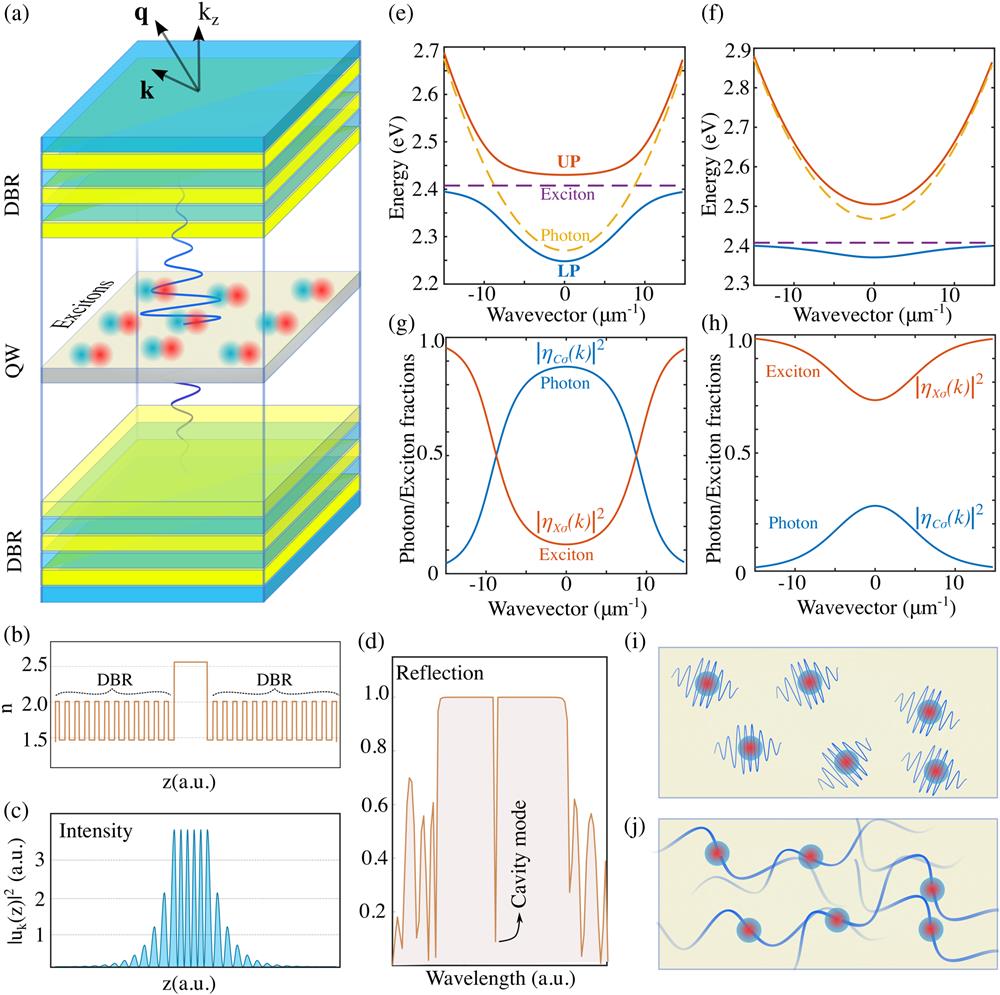
    Fig. 1. Fundamentals of microcavity exciton polaritons. (a) Schematic of a semiconductor microcavity, which consists of two distributed Bragg reflector (DBR) mirrors and a semiconductor quantum well (QW). The photons trapped inside the cavity formed by the DBR mirrors interact with the excitons (electron–hole pairs) in the QW. (b) Example of the schematic variation of refractive index n along the growth direction (z axis) of a microcavity. The periodic variation of low and high values of the refractive index forms a DBR. Two face-to-face periodic structures (DBRs) form a cavity where the QW (here with a higher refractive index) is embedded. (c) Intensity distribution |uk(z)|2 along the z axis of the photonic mode trapped inside the cavity. (d) Reflection from the microcavity, which shows a stop band (flat region where the reflection is almost one) and a cavity mode as indicated in the figure. (e), (f) Dispersion of upper (UP) and lower (LP) polariton modes (solid lines), which emerge from the strong coupling between photons (yellow dotted line) and excitons (purple dotted line) for different detunings between excitons and the cavity mode. (g), (h) Exciton (|η(k)|2) and photon (|η(k)|2) fractions of the lower polariton mode as functions of the wave vector for different detunings between excitons and the cavity mode. These fractions are given by the Hopfield coefficients η(k) and η(k). (i) Classical Bose gas with the average interparticle distance much larger than the thermal de Broglie wavelength (λT). (j) Quantum gas (Bose–Einstein condensate) with the average interparticle distance comparable to λT.
    Commonly used experimental methods. (a) Schematic of the angle-resolved photoluminescence setup with Fourier image configuration[35]. (b) Top, schematic of the Michelson interferometer setup. Bottom, illustration of centro-symmetrically interfered images.
    Fig. 2. Commonly used experimental methods. (a) Schematic of the angle-resolved photoluminescence setup with Fourier image configuration[35]. (b) Top, schematic of the Michelson interferometer setup. Bottom, illustration of centro-symmetrically interfered images.
    Applications of microcavity exciton polaritons. (a) Angle resolved photoluminescence below threshold (left), at threshold (middle), and above threshold (right). The polariton condensate above threshold acts as a polariton laser[122]. (b) Lattice simulator for realizing topological insulator using exciton polaritons under a strong magnetic field[134]. (c) Left: schematic of a room temperature lattice simulator using intrinsic anisotropy of perovskite microcavities. Right: eigenvalues in trivial (W = 0) and topological (W = 1) phases of the simulated Su–Schrieffer–Heeger model[135]. (d) Top: scheme of an all-optical polariton transistor. Bottom: real space emission image of address beams A and B and control beam C[14]. (e) Top: schematic representation of a polariton neuromorphic computer for handwritten digit recognition. Bottom: experimental scheme of modulating a laser beam with spatial light modulator (SLM) and a CCD camera to get the output[161]. (f) Left: proposal for realizing qubits using quantum fluctuations in polariton condensates. Right: fidelities of polariton quantum gates (SWAP and sSWAP) as functions of lifetime compared to the interaction strength[168].
    Fig. 3. Applications of microcavity exciton polaritons. (a) Angle resolved photoluminescence below threshold (left), at threshold (middle), and above threshold (right). The polariton condensate above threshold acts as a polariton laser[122]. (b) Lattice simulator for realizing topological insulator using exciton polaritons under a strong magnetic field[134]. (c) Left: schematic of a room temperature lattice simulator using intrinsic anisotropy of perovskite microcavities. Right: eigenvalues in trivial (W = 0) and topological (W = 1) phases of the simulated Su–Schrieffer–Heeger model[135]. (d) Top: scheme of an all-optical polariton transistor. Bottom: real space emission image of address beams A and B and control beam C[14]. (e) Top: schematic representation of a polariton neuromorphic computer for handwritten digit recognition. Bottom: experimental scheme of modulating a laser beam with spatial light modulator (SLM) and a CCD camera to get the output[161]. (f) Left: proposal for realizing qubits using quantum fluctuations in polariton condensates. Right: fidelities of polariton quantum gates (SWAP and sSWAP) as functions of lifetime compared to the interaction strength[168].
    Exciton polaritons in GaN microcavities and ZnO microcavities. (a) GaN polariton lasing at room temperature[31]. Top left panel: bulk GaN microcavity (inset) and reflectivity at 300 K with lower polariton mode marked by the arrow. Bottom left panel: theoretical simulation of polariton dispersion. Right top and bottom panels: photoluminescence spectra as a function of pump power (20 μW to 2 mW). (b) Electrical injection GaN-based microcavity diode polariton lasing at room temperature[210]. Top left panel: schematic image of GaN-based microcavity diode. Top right panel: measured data (black dot) of polariton dispersion simulated by a coupled harmonic oscillator model. Bottom left panel: angle-resolved electroluminescence showing the polariton condensation at ground state at high current injection densities. Bottom right panel: transition from polariton lasing to photon lasing. (c) Polariton parametric scattering (PPS) in ZnO microcavity at room temperature[222]. Top left panel: scanning electron microscope (SEM) image of ZnO microwire with whispering gallery modes. Top right panel: multiple lower polariton modes along TE polarization (left image) and TM polarization (right image). Bottom left panel: polariton lasing in the ZnO microcavity at pumping power of 0.33 μW. Bottom middle panel: polariton parametric scattering in the ZnO microcavity at pumping power of 1.3 μW. Bottom right panel: schematic diagram of the PPS between the adjacent polariton branches. (d) Weak lasing in one-dimensional ZnO-Si polariton superlattices at room temperature[29]. Top left panel: SEM image of ZnO microwire placed on a periodic Si grating. Top right panel: folded polariton dispersion caused by a polariton superlattice. Bottom left panel: polariton lasing at the excited polariton states (edges of the Brillouin zone). Bottom right panel: spatially resolved photoluminescence showing the emission spots settled in the periodic potential.
    Fig. 4. Exciton polaritons in GaN microcavities and ZnO microcavities. (a) GaN polariton lasing at room temperature[31]. Top left panel: bulk GaN microcavity (inset) and reflectivity at 300 K with lower polariton mode marked by the arrow. Bottom left panel: theoretical simulation of polariton dispersion. Right top and bottom panels: photoluminescence spectra as a function of pump power (20 μW to 2 mW). (b) Electrical injection GaN-based microcavity diode polariton lasing at room temperature[210]. Top left panel: schematic image of GaN-based microcavity diode. Top right panel: measured data (black dot) of polariton dispersion simulated by a coupled harmonic oscillator model. Bottom left panel: angle-resolved electroluminescence showing the polariton condensation at ground state at high current injection densities. Bottom right panel: transition from polariton lasing to photon lasing. (c) Polariton parametric scattering (PPS) in ZnO microcavity at room temperature[222]. Top left panel: scanning electron microscope (SEM) image of ZnO microwire with whispering gallery modes. Top right panel: multiple lower polariton modes along TE polarization (left image) and TM polarization (right image). Bottom left panel: polariton lasing in the ZnO microcavity at pumping power of 0.33 μW. Bottom middle panel: polariton parametric scattering in the ZnO microcavity at pumping power of 1.3 μW. Bottom right panel: schematic diagram of the PPS between the adjacent polariton branches. (d) Weak lasing in one-dimensional ZnO-Si polariton superlattices at room temperature[29]. Top left panel: SEM image of ZnO microwire placed on a periodic Si grating. Top right panel: folded polariton dispersion caused by a polariton superlattice. Bottom left panel: polariton lasing at the excited polariton states (edges of the Brillouin zone). Bottom right panel: spatially resolved photoluminescence showing the emission spots settled in the periodic potential.
    Exciton polariton condensate and superfluidity in OSC microcavities. (a) Left: schematic of the microcavity and anthracene crystal structure. Right: calculated dispersion along the a-crystal axis showing the formation of LP branch, UP branch, and two middle branches arising from strong coupling of intramolecular vibronic modes, as indicated in the absorption spectrum[33]. (b) Left top and bottom: DBR microcavity and chemical structure of the MeLPPP polymer. Top middle and right: momentum resolved map for excitation power below (middle) and above threshold (right). Bottom middle and right: same as in the top panel but for real space emission. The insets show the g(1) interferograms. Scale bars are 20 µm[176]. (c) Top left and right: g(1) maps for increasing pumping fluence. Scale bars are 5 µm. Bottom left and right: vertical cuts of the g(1) maps reported in the top panel[250]. (d) Left: sketch of the optical setup and microcavity embedding TDAF. Top middle and right: real space emission for low (middle) and high polariton density (right). Bottom middle and right: same as in the top panel but for the momentum space emission[6].
    Fig. 5. Exciton polariton condensate and superfluidity in OSC microcavities. (a) Left: schematic of the microcavity and anthracene crystal structure. Right: calculated dispersion along the a-crystal axis showing the formation of LP branch, UP branch, and two middle branches arising from strong coupling of intramolecular vibronic modes, as indicated in the absorption spectrum[33]. (b) Left top and bottom: DBR microcavity and chemical structure of the MeLPPP polymer. Top middle and right: momentum resolved map for excitation power below (middle) and above threshold (right). Bottom middle and right: same as in the top panel but for real space emission. The insets show the g(1) interferograms. Scale bars are 20 µm[176]. (c) Top left and right: g(1) maps for increasing pumping fluence. Scale bars are 5 µm. Bottom left and right: vertical cuts of the g(1) maps reported in the top panel[250]. (d) Left: sketch of the optical setup and microcavity embedding TDAF. Top middle and right: real space emission for low (middle) and high polariton density (right). Bottom middle and right: same as in the top panel but for the momentum space emission[6].
    Plasmonic systems coupled with OSCs. (a) Left: schematic of a methylene-blue molecule in the gap of a plasmonic nanoparticle-on-mirror geometry. Right: scattering spectra of isolated nanoparticles with the transition dipole moment parallel (top) and perpendicular to the mirror (bottom)[78]. (b) Left top and bottom: schematic of the nanoparticle array covered with dye molecules and corresponding absorption and emission spectra of the rylene dye in PMMA. Right top and bottom: experimental g(1) interferogram (top) and map of g(1) correlation function (bottom)[72,275].
    Fig. 6. Plasmonic systems coupled with OSCs. (a) Left: schematic of a methylene-blue molecule in the gap of a plasmonic nanoparticle-on-mirror geometry. Right: scattering spectra of isolated nanoparticles with the transition dipole moment parallel (top) and perpendicular to the mirror (bottom)[78]. (b) Left top and bottom: schematic of the nanoparticle array covered with dye molecules and corresponding absorption and emission spectra of the rylene dye in PMMA. Right top and bottom: experimental g(1) interferogram (top) and map of g(1) correlation function (bottom)[72,275].
    BEC under quasi-CW pumping, polariton devices, and topological polariton lasing in OSCs. (a) Left top and bottom: schematic of the eGFP molecular structure (top) and corresponding molecular arrangement in solid state (bottom). Top left, middle, and right: momentum space map for excitation power below (left), at threshold (middle), and above threshold (right). Bottom: two thresholds behavior and transition from polariton lasing to photonic lasing[276]. (b) Left: schematic of the MeLPPP microcavity and pumping scheme. The pump is tuned one vibron above the control beam (ground state). Top: schematic of the polariton transistor. Bottom left and right: schematic of the first amplification stage (left) and second amplification stage (right) demonstrating the cascadability[15]. (c) Left: ground state stimulated polariton population by decreasing the seed power (from top to bottom). Right: total population triggered by 2.7 (top) and one photon per pulse (bottom)[279]. (d) Top: schematic of the Su–Schrieffer–Heeger chain; red dots indicate the boundary and edge defects. Middle panel: below threshold energy-resolved momentum space collected by exciting the bulk of the chain (left) and the boundary defect (middle). The corresponding real space emission including the boundary defect is reported in the right map. Bottom: above threshold energy-resolved momentum space collected by exciting the boundary defect (left). The corresponding real space interferogram and g(1) correlation function including the boundary defect are reported in the right-top and right-bottom images, respectively[293].
    Fig. 7. BEC under quasi-CW pumping, polariton devices, and topological polariton lasing in OSCs. (a) Left top and bottom: schematic of the eGFP molecular structure (top) and corresponding molecular arrangement in solid state (bottom). Top left, middle, and right: momentum space map for excitation power below (left), at threshold (middle), and above threshold (right). Bottom: two thresholds behavior and transition from polariton lasing to photonic lasing[276]. (b) Left: schematic of the MeLPPP microcavity and pumping scheme. The pump is tuned one vibron above the control beam (ground state). Top: schematic of the polariton transistor. Bottom left and right: schematic of the first amplification stage (left) and second amplification stage (right) demonstrating the cascadability[15]. (c) Left: ground state stimulated polariton population by decreasing the seed power (from top to bottom). Right: total population triggered by 2.7 (top) and one photon per pulse (bottom)[279]. (d) Top: schematic of the Su–Schrieffer–Heeger chain; red dots indicate the boundary and edge defects. Middle panel: below threshold energy-resolved momentum space collected by exciting the bulk of the chain (left) and the boundary defect (middle). The corresponding real space emission including the boundary defect is reported in the right map. Bottom: above threshold energy-resolved momentum space collected by exciting the boundary defect (left). The corresponding real space interferogram and g(1) correlation function including the boundary defect are reported in the right-top and right-bottom images, respectively[293].
    Exciton polaritons in perovskite microcavities. (a) Left panel: schematic of CsPbCl3 perovskite microcavity, consisting of a CsPbCl3 perovskite layer and HfO2/SiO2 top and bottom DBRs. Middle panel: exciton polariton dispersion of the CsPbCl3 perovskite microcavity, showing the strong coupling regime. Right panel: exciton polariton condensation spectrum of the CsPbCl3 perovskite microcavity[35]. (b) Left panel: schematic of 1D CsPbBr3 microcavity. Middle panel: optical and fluorescence images of the 1D CsPbBr3 microcavity. Right panel: real space image of the propagating polariton condensate, showing long-range propagation up to 60 µm[36]. (c) Left panel: schematic of the (C6H5C2H4NH3)2PbI4 perovskite microcavity, consisting of a (C6H5C2H4NH3)2PbI4 perovskite layer, bottom DBR, and silver top mirror. Middle panel: exciton polariton dispersion below threshold. Right panel: exciton polariton dispersion above threshold[184]. (d) Left panel: atomic force microscopy image of the 1D perovskite lattice. Middle panel: exciton polariton dispersion of the CsPbBr3 lattice below threshold, showing a large gap opening of 13 meV. Right panel: exciton polariton dispersion of the CsPbBr3 perovskite lattice above threshold, showing condensation at py orbital state[47].
    Fig. 8. Exciton polaritons in perovskite microcavities. (a) Left panel: schematic of CsPbCl3 perovskite microcavity, consisting of a CsPbCl3 perovskite layer and HfO2/SiO2 top and bottom DBRs. Middle panel: exciton polariton dispersion of the CsPbCl3 perovskite microcavity, showing the strong coupling regime. Right panel: exciton polariton condensation spectrum of the CsPbCl3 perovskite microcavity[35]. (b) Left panel: schematic of 1D CsPbBr3 microcavity. Middle panel: optical and fluorescence images of the 1D CsPbBr3 microcavity. Right panel: real space image of the propagating polariton condensate, showing long-range propagation up to 60 µm[36]. (c) Left panel: schematic of the (C6H5C2H4NH3)2PbI4 perovskite microcavity, consisting of a (C6H5C2H4NH3)2PbI4 perovskite layer, bottom DBR, and silver top mirror. Middle panel: exciton polariton dispersion below threshold. Right panel: exciton polariton dispersion above threshold[184]. (d) Left panel: atomic force microscopy image of the 1D perovskite lattice. Middle panel: exciton polariton dispersion of the CsPbBr3 lattice below threshold, showing a large gap opening of 13 meV. Right panel: exciton polariton dispersion of the CsPbBr3 perovskite lattice above threshold, showing condensation at py orbital state[47].
    Topological and non-Hermitian effects in perovskite microcavities. (a) Left panel: exciton polariton dispersion below threshold at 0 T and 9 T. Middle panel: Berry curvature distribution at 0 T. Right panel: normalized maximal Berry curvature value as a function of the magnetic field[311]. (b) Left panel: schematic of the two exceptional points connected by the bulk Fermi arc. Middle panel: texture of circular polarization near the two pairs of exceptional points. Right panel: spectral phase winding near the exceptional points, showing fractional topological charge[10].
    Fig. 9. Topological and non-Hermitian effects in perovskite microcavities. (a) Left panel: exciton polariton dispersion below threshold at 0 T and 9 T. Middle panel: Berry curvature distribution at 0 T. Right panel: normalized maximal Berry curvature value as a function of the magnetic field[311]. (b) Left panel: schematic of the two exceptional points connected by the bulk Fermi arc. Middle panel: texture of circular polarization near the two pairs of exceptional points. Right panel: spectral phase winding near the exceptional points, showing fractional topological charge[10].
    Coupling in TMD nanocavities. (a) Left panel: schematic of the planar microcavity. Right panel: angle-resolved photoluminescence (PL) spectra of the TMD microcavity[37]. (b) Left panel: schematic diagram of a monolayer WSe2 under alumina coating and a single silver nanorod. Right panel: dark-field scattering spectra of the silver nanorod with an increased alumina coating (top). Energy of the UPB and LPB as a function of detuning, giving a splitting of 49.5 meV[68]. (c) Top panel: absorption spectrum of monolayer WS2. Middle panel: dark-field scattering spectrum of a plasmonic nanogap resonator. Bottom panel: scattering spectrum of a monolayer WS2 embedded in a plasmonic nanogap resonator[64]. (d) Left panel: schematic diagram of the coupling of out-of-plane dipole of dark exciton and the plasmon mode. Right panel: PL spectra for a single etched WSe2-NPoM nanocavity. Peaks at 1.6 eV and 1.66 eV correspond to the emission of dark exciton and bright exciton, respectively[76].
    Fig. 10. Coupling in TMD nanocavities. (a) Left panel: schematic of the planar microcavity. Right panel: angle-resolved photoluminescence (PL) spectra of the TMD microcavity[37]. (b) Left panel: schematic diagram of a monolayer WSe2 under alumina coating and a single silver nanorod. Right panel: dark-field scattering spectra of the silver nanorod with an increased alumina coating (top). Energy of the UPB and LPB as a function of detuning, giving a splitting of 49.5 meV[68]. (c) Top panel: absorption spectrum of monolayer WS2. Middle panel: dark-field scattering spectrum of a plasmonic nanogap resonator. Bottom panel: scattering spectrum of a monolayer WS2 embedded in a plasmonic nanogap resonator[64]. (d) Left panel: schematic diagram of the coupling of out-of-plane dipole of dark exciton and the plasmon mode. Right panel: PL spectra for a single etched WSe2-NPoM nanocavity. Peaks at 1.6 eV and 1.66 eV correspond to the emission of dark exciton and bright exciton, respectively[76].
    Valley polaritons. (a) Left panel: schematic of the valley-polarized polaritons, consisting of monolayer MoS2 strongly coupled to a planar microcavity. Right panel: emission spectra of polaritons excited by left and right circular polarized light at 8 and 294 K[348]. (b) Left panel: sketch of polarization-dependent transient reflectance measurements of WS2 polariton in microcavity (top); schematic of valley-dependent optical selection rules at the band edges (bottom). Right panel: valley-selective shift of highly detuned polaritons at room temperature[353].
    Fig. 11. Valley polaritons. (a) Left panel: schematic of the valley-polarized polaritons, consisting of monolayer MoS2 strongly coupled to a planar microcavity. Right panel: emission spectra of polaritons excited by left and right circular polarized light at 8 and 294 K[348]. (b) Left panel: sketch of polarization-dependent transient reflectance measurements of WS2 polariton in microcavity (top); schematic of valley-dependent optical selection rules at the band edges (bottom). Right panel: valley-selective shift of highly detuned polaritons at room temperature[353].
    Polariton devices. (a) Left panel: device schematic and tunneling mechanism. Right panel: angle-resolved reflectance (top) and electroluminescence (bottom)[364]. (b) Top panel: schematic of BSWPs (left); angle-resolved reflection spectra of the BSW polaritons (right). Bottom panel: power sweep of the LP branch for the highest exciton fraction (left); nonlinear polariton source at an exciton fraction of 36%, red and blue curves show the normalized intensity of scattered and propagating beams, which have a super-linear dependence on pump fluence (right)[193]. (c) Left panel: angle-resolved reflection spectra, demonstrating the formation of the idler state. Right panel: triggered parametric scattering observed at room temperature. The orange and purple lines represent the transmission spectra of seed alone and seed with pump, respectively. The gain as a function of pump fluence is shown in the inset[196]. (d) Observation of WS2 microcavity polariton lasing at room temperature. Left panel: above-threshold angle-resolved PL spectra. Right panel: visibility as a function of time delay when the pump power is kept above the threshold. The top left inset shows a schematic diagram of the microcavity structure. The top right inset shows the interference pattern visible at Δt = 0 ps[120].
    Fig. 12. Polariton devices. (a) Left panel: device schematic and tunneling mechanism. Right panel: angle-resolved reflectance (top) and electroluminescence (bottom)[364]. (b) Top panel: schematic of BSWPs (left); angle-resolved reflection spectra of the BSW polaritons (right). Bottom panel: power sweep of the LP branch for the highest exciton fraction (left); nonlinear polariton source at an exciton fraction of 36%, red and blue curves show the normalized intensity of scattered and propagating beams, which have a super-linear dependence on pump fluence (right)[193]. (c) Left panel: angle-resolved reflection spectra, demonstrating the formation of the idler state. Right panel: triggered parametric scattering observed at room temperature. The orange and purple lines represent the transmission spectra of seed alone and seed with pump, respectively. The gain as a function of pump fluence is shown in the inset[196]. (d) Observation of WS2 microcavity polariton lasing at room temperature. Left panel: above-threshold angle-resolved PL spectra. Right panel: visibility as a function of time delay when the pump power is kept above the threshold. The top left inset shows a schematic diagram of the microcavity structure. The top right inset shows the interference pattern visible at Δt = 0 ps[120].
    Exciton polaritons in single-walled carbon nanotube (SWCNT) microcavities. (a) Near-infrared exciton polaritons in SWCNT microcavities. Left panel: SWCNT/PFO-BPy embedded in an Au cavity measured by angle-resolved spectroscopy setup. Middle panel: angle-resolved reflectivity (left image) and photoluminescence (right image). Right panel: reflectivity and PL of SWCNT-filled cavity versus cavity thickness[38]. (b) Electrical injection and tuning of exciton polaritons in SWCNT microcavities. Left panel: schematic image of single-walled carbon nanotube-based light-emitting field-effect transistors. Middle panel: angle-resolved photoluminescence (left image) and electroluminescence (right image). Right panel: reflectivity displaying Rabi splitting changed at four different gate voltages[39]. (c) Transition between weak and ultra-strong coupling of exciton polariton via exceptional points in SWCNT microcavity. Left panel: schematic geometry of the aligned SWCNT microcavity. Middle panel: anisotropic polariton dispersions along parallel (φ = 0°) and perpendicular (φ = 90°) polarizations. Right panel: two pairs of exceptional points obtained in the upper polariton (UP) and lower polariton (LP) dispersion surfaces (left image); real (top) and imaginary (bottom) parts of eigenfrequencies changing with coupling strength (ħg) (right image)[40].
    Fig. 13. Exciton polaritons in single-walled carbon nanotube (SWCNT) microcavities. (a) Near-infrared exciton polaritons in SWCNT microcavities. Left panel: SWCNT/PFO-BPy embedded in an Au cavity measured by angle-resolved spectroscopy setup. Middle panel: angle-resolved reflectivity (left image) and photoluminescence (right image). Right panel: reflectivity and PL of SWCNT-filled cavity versus cavity thickness[38]. (b) Electrical injection and tuning of exciton polaritons in SWCNT microcavities. Left panel: schematic image of single-walled carbon nanotube-based light-emitting field-effect transistors. Middle panel: angle-resolved photoluminescence (left image) and electroluminescence (right image). Right panel: reflectivity displaying Rabi splitting changed at four different gate voltages[39]. (c) Transition between weak and ultra-strong coupling of exciton polariton via exceptional points in SWCNT microcavity. Left panel: schematic geometry of the aligned SWCNT microcavity. Middle panel: anisotropic polariton dispersions along parallel (φ = 0°) and perpendicular (φ = 90°) polarizations. Right panel: two pairs of exceptional points obtained in the upper polariton (UP) and lower polariton (LP) dispersion surfaces (left image); real (top) and imaginary (bottom) parts of eigenfrequencies changing with coupling strength (ħg) (right image)[40].
    Material TypeExcitonMaterialMorphologySynthesisEg at 300 K (eV)Eb(meV)Rabi Splitting (meV)Ref.
    Traditional inorganicWannier–MottGaNBulkMBE3.422531–60[31]
    QWMOVPE3–3.34017–56[173]
    MicrowireMOVPE3.4225115[174]
    Wannier–MottZnOMicrowireCarbothermal method3.3160200–330[29]
    BulkPLD3.316050–260[30]
    Traditional organicFrenkelJ-aggregatesFilmSolution method1.836080-160[32]
    AnthraceneSingle crystalMelt-grown method3.1664086–256[33]
    TDAFFilmThermal evaporation3.5NA600–1000[175]
    Conjugated polymerFilmSpin-coating2.7116[176]
    Halide perovskitesWannier–Mott(PEA)2PbX4 (X=I, Br, Cl)Film/flakeSpin-coating/exfoliation2.3–3.1420090–230[177184]
    MAPbBr3FilmSpin-coating2.33070[185]
    NanowireSolution method2.3390[186]
    CsPbBr3NanoplateletCVD2.40740120[36,47,99,100,187]
    NanowireSolution method2.407200[142,188]
    CsPbCl3NanoplateletCVD3.0470270[35,189]
    (BA)2(MA)n1PbnI3n+1 (n=15)CrystalExfoliation1.56–2.55125–470NA[190,191]
    Transition metal dichalcogenidesWannier–MottMX2 (M=Mo, W;X=S, Se)FlakeExfoliation/CVD1–2320–72011.4–780[37,120,192196]
    Carbon nanotubesWannier–MottSingle-walled carbon nanotubes (SWCNTs)SWCNTs in thin polymer filmSolution method0–2300–50035–127[3840,197,198]
    Table 1. Comparison of Room Temperature Polariton Semiconductor Systems.
    Sanjib Ghosh, Rui Su, Jiaxin Zhao, Antonio Fieramosca, Jinqi Wu, Tengfei Li, Qing Zhang, Feng Li, Zhanghai Chen, Timothy Liew, Daniele Sanvitto, Qihua Xiong. Microcavity exciton polaritons at room temperature[J]. Photonics Insights, 2022, 1(1): R04
    Download Citation