
Alessio Buzzin, Rita Asquini, Domenico Caputo, Giampiero de Cesare. Evanescent waveguide lab-on-chip for optical biosensing in food quality control[J]. Photonics Research, 2022, 10(6): 1453
- Photonics Research
- Vol. 10, Issue 6, 1453 (2022)
Abstract
1. INTRODUCTION
Nowadays, growing efforts are made worldwide to address food quality issues. Pollution, consumer awareness, as well as human overpopulation motivate the need of deep studies in this field: the main goals are to set food quality standards, to better comprehend health risks, and to expose deceptions due to adulteration and contamination phenomena [1]. Food adulteration can be either intentional or unintentional and can take many forms, such as the addition of sugars or toxic products, metallic or microbial contamination, and overdilution of concentrate [2]. The increasing need for high-quality natural food with clear origin pushes modern technology to develop sensing procedures and intensely investigate this topic: although chemical/electrochemical methods are often employed in this field [3,4], spectroscopic [5–7] and refractive index [8] investigations play an important role in the safety and quality monitoring of drinks and beverages [9] as well as wine [10], oils [11], and dairy products [12]. Optical investigations trends for food quality control are focused on the development of portable, highly integrated, and cost-effective devices, relying on colorimetry [13], imaging [14,15], surface plasmon resonance [16,17], or taking advantage of optical absorption [18], fluorescence [19,20], evanescent waves [21], and refractive index variations [22–24]. Nevertheless, current optical biosensing methods are still generally articulated in separated components: light source, sample handle treatment, and detector [25].
This paper introduces a compact, inexpensive, and easy-to-use device that integrates in a single glass chip the optical interaction with the sample and the detection phases. The device is able to sense a variation in the complex refractive index of a liquid mixture and link it to the change of a specific feature, such as the concentration of an analyte. The basic operating principle relies on exploitation of the well-known waveguide evanescent field sensing mechanism, based on the interaction of the evanescent tail of a waveguided mode with neighboring media: a refractive index variation of a sample droplet on the waveguide surface changes the mode effective refractive index through the evanescent field, and allows for a quantitative measurement of the substance [26,27]. Preliminary configurations were recently explored with the same operating principle, and the general concept was theoretically proven for biomedical applications [28,29]. Here we come up with a complete and fully functional system, able to act as an optical biosensor suitable for food quality monitoring when anomalies such as overdilution by water addition need to be detected. The device allows non-destructive inspection, without the need of sample pre-treatment with hazardous chemicals, requiring small sample volumes and thus reducing sample wastage. In our concept, a glass substrate hosts a plastic microfluidic structure that allows interaction between the biological sample and an SU-8 polymer optical waveguide; the traveling light is routed to a thin-film hydrogenated amorphous silicon (a-Si:H) photodiode to perform on-chip detection of the sample’s analyte concentration. The following sections present the system’s design, working principle and targets, a description of the fabrication process, the electro-optical characterization of a first prototype, a numerical analysis of a possible application scenario involving milk quality assessment, and an experimental campaign to check and confirm the device’s biosensing performances.
2. OPERATION MODE AND DESIGN
The proposed sensor is an on-glass integrated system able to evaluate the analyte’s concentration inside a biological sample by detecting variations of the sample’s refractive index, exploiting the evanescent wave phenomenon. The device embeds two main sections: the interaction site and the detection site. The former is a combination of an optical channel and a microfluidic structure, while the latter consists of an embedded photosensor, optically coupled with the waveguide, that performs on-chip detection when light variations occur. The operations start when coherent light is routed into the system’s waveguide and driven to the interaction site. The sample is then placed in the interaction site. Due to the evanescent wave phenomenon, the sample absorbs part of the traveling light: variations of the analyte’s concentration lead to changes in the real () and imaginary () parts of the sample’s refractive index; thus, the optical absorption in the interaction site changes accordingly. Light changes are detected by the embedded photodiode: monitoring the amplitude shifts in the photogenerated currents, the user can trace back the optical properties of the sample and, finally, the analyte’s concentration values. Figure 1 depicts the proposed system.
Sign up for Photonics Research TOC. Get the latest issue of Photonics Research delivered right to you!Sign up now
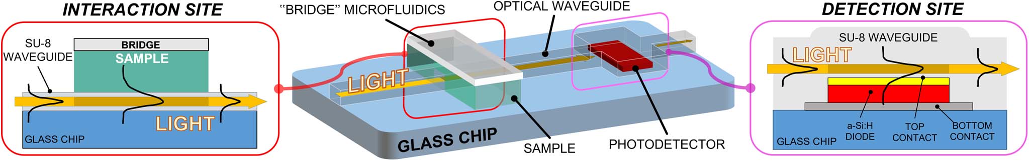
Figure 1.Evanescent waveguide lab-on-chip basic structure, with two sectioned insights on the sample–waveguide interaction site (left side) and on the waveguide–photosensor detection site (right site).
A. Interaction Site
For this kind of application, the optical waveguide must be biocompatible to avoid biological adulterations and must present a certain technological versatility to allow its fabrication on substrates of different kinds (glass, plastic, silicon); moreover, for mass production purposes, it must be inexpensive and easy to manufacture. To suit the requirements, our choice for the waveguiding material was SU-8, a photosensitive polymer that can be patterned by means of UV photolithography on a variety of substrates [30]. The versatility and biocompatibility of SU-8 allow its use in different applications, from micro-electromechanical systems (MEMS) [31] and microelectronics [32] to medicine [33]. SU-8 has a consolidated and well-known reference as waveguiding structure, due to its high refractive index and low optical losses in a wide range of frequencies [34].
As part of the interaction site, the microfluidic structure needs to satisfy specific requirements. First, other than being biocompatible, it must convey the biological sample over the optical channel without interfering with the sample–waveguide interaction. Moreover, it must be inexpensive, rapid, and simple to manufacture and integrate. For these purposes, pressure-sensitive adhesives (PSAs) were chosen as biocompatible, medical-grade plastic materials, resistant to chemicals, flexible, and transparent [35]. PSAs are often employed to create 3D microfluidic structures for biomedical applications [36] through a razor-cutting prototyping technique (or “xurography”), with the help of a cutting plotter [37]. A suspended, bridge-shaped structure has been specifically designed to confine the sample–waveguide interaction, avoiding any other material in direct contact with the waveguide and to prevent any perturbation or anomaly in the light travel. The structure is also easy to fill with the biological sample, due to capillary forces. The confinement of the interaction area gives a clear advantage in reaching more stable and reproducible measures with respect to a less accurate and randomly placed sample droplet. To optimize the optical absorption, the sample–waveguide contact surface can be modified by tuning the thickness and width of the optical channel, as well as the overlapping area’s length, as reported in previous investigations [29].
To study the waveguide-to-sample optical absorption, the interaction site (see Fig. 1) was longitudinally sectioned and modeled with COMSOL Multiphysics using the “Electromagnetic Waves Frequency Domain” module. The “sample” domain was modeled taking into consideration the optical properties of biological samples whose refractive indices change according to specific analyte concentrations. Figure 2 shows the simulated results achieved using the values of milk’s refractive index at different fat concentrations taken from literature [38]. Figure 2(a) shows the investigated section and the evolution of the electromagnetic field from left (“in” box) to right (“out” box) when the light excitation comes from the left edge of the waveguide domain. The evaluated amount of optical power absorbed by the samples is plotted in Fig. 2(b) as a function of the optical properties ( and ) of the samples. The reported simulations were performed at a 660 nm wavelength, considering a BK7 glass substrate with a refractive index equal to 1.52 (as reported by SCHOTT optical glasses data sheets), and a 5-μm-thick SU-8 waveguide with a refractive index equal to 1.58 (as reported in MICROCHEM’s SU-8 3000 data sheet). Results confirm that different refractive indices bring to different waveguide-to-sample optical absorptions. Therefore, the light exiting the interaction site is a useful tool to mark the sample’s refractive index and, ultimately, the analyte concentration inside the sample.
![]()
Figure 2.(a) Modeled optical power absorption in the longitudinal section of the interaction site by a biological sample, with a 4-mm-long sample–waveguide overlap. (b) Evaluated optical power absorption versus samples’ complex refractive indices (
B. Detection Site
To perform a transduction from optical power to electric current, the system must include a photodetector. The hybrid nature of the device forces the coexistence of different materials such as glass and polymers, requiring technological versatility for the detector to be embedded in such a system. Moreover, the overall performances depend on the detector’s electro-optical responsivity (R), sensitivity (S), and limit of detection (LoD). A thin-film, p-doped/intrinsic/n-doped photodiode made of a-Si:H was chosen as the optical detector. The device’s integrability is guaranteed by its low-temperature fabrication procedure, usually by plasma enhanced chemical vapor deposition (PECVD), which allows compatibility not only with the standard silicon CMOS framework, but also with other substrates, such as glass or flexible polymers [39]. Amorphous silicon p-type-intrinsic-n-type (p-i-n) photodiodes provide high electro-optical R and high quantum efficiency across the visible spectrum; moreover, they present a low dark current and, therefore, a low LoD [40]. These unique features made a-Si:H popular over the years as key material mainly in applications where low cost, large areas, and high performances are required, such as sensing [41] and photovoltaics [42], and be currently under study as waveguides in silicon photonics devices [43].
The two junctions’ doped layers provide the device’s built-in electric potential, while the intrinsic layer represents the junctions’ physical depletion regions and active areas. The thickness of the intrinsic layer has been designed to widen the photoresponse across the whole visible spectrum and, at the same time, to reduce the dark current due to the higher energy gap [44]. Light impinges on the device’s top layer, whose thickness must be carefully designed to enhance the optical transmission of the visible spectrum wavelengths to the intrinsic layer. Consequently, thicknesses of 50 nm, 500 nm, and 10 nm were chosen for the n-i-p layers, respectively. Furthermore, the n-i-p sequence assures the growth of a more stable and performing device in terms of process temperature, allowing a transition from 200°C for n-type deposition to 180°C for the intrinsic layer, and finally to 150°C for p-type deposition.
To extract the photocurrent signal, electrical connection to the external electronics is provided. For the p-side, the electrical contact must also be optically transparent. Transparent conductive oxides (TCOs), such as indium–tin oxide (ITO), are employed in a variety of applications where both electrical conductivity and optical transparency are required, such as solar cells or displays [45], as well as integrated photonic devices [46]. The choice of ITO is also supported by its technological compatibility with device fabrication. Chromium (Cr) was chosen for the n-side contact, while a titanium–tungsten (Ti/W) metallic alloy film was used for the metal interconnections.
As a protection from the external environment and from short circuits, the junction stack is surrounded by an electrical insulator that, at the same time, must not adulterate the optical information nor its transduction into electric signal. This issue was addressed by considering SU-8 with the purpose of providing electrical insulation while delivering traveling light to the detector. Both tasks can be accomplished by overlapping the junction stack through a single SU-8 photolithographic step. Similar attempts were made in the past to optically couple silicon structures and SU-8 waveguides [47], encouraging further developments and actual implementations.
In previous investigations, a BK7 ion-diffused waveguiding structure was developed with a p-i-n photodiode over the optical channel: several studies and attempts were made to successfully perform the routing of light through the bottom of the diode and the coupling between the two components [28]. In our case, the overlapped configuration, with the SU-8 waveguide above the photosensor, assures the growth of a-Si:H on glass, with superior adhesion and smoother interfaces with respect to the growth on SU-8.
To investigate the optical coupling between detector and waveguide, the photodiode’s material stack including the ITO layer was simulated with COMSOL Multiphysics. The upper part of Fig. 2(c) shows a section of the detection site, while the lower part shows the evolution of the optical power inside the waveguide from left (in box) to right (out box) [similar to Fig. 2(a)]. Figure 2(d) plots the coupling efficiency, evaluated as and normalized to its maximum, as a function of the ITO top contact thickness: when light excitation is at 532 nm wavelength, a peak is reached at around 120 nm thickness.
3. PROTOTYPING
A. Device Fabrication
Different configurations were investigated for this kind of system, whose manufacturing procedure has been extensively described in previous works [28,29]. Thin-film microelectronic technologies were used to assemble a prototype, with a total of four lithographic steps for the presented configuration. The overall system was fabricated inside a area. Figure 3(a) shows a picture of the assembled prototype; Fig. 3(b) displays a microscope enlargement on the detection site, with geometry details.
![]()
Figure 3.(a) Fabricated system. (b) Enlarged top view of the fabricated detector.
B. Prototype Characterization
To obtain the current–voltage (I-V) curve of the photodiode, the fabricated prototype was electrically connected to a Keithley 236 Source-Measure Unit (SMU, from Keithley Instruments, Ohio, USA), and a voltage sweep was performed from to 1 V in dark conditions. As a result, the sensor under test (with a surface area of ) showed a dark current density of about at a small reverse bias (), with a corresponding Schottky noise current contribution of about . The detector’s quantum efficiency in the visible spectrum was measured on a reference sensor, with a larger area to fit the specific requirements of our optical setup R. The complete to 1 V current density versus bias voltage curves, for both sensors, are plotted in Fig. 4. The two curves are almost completely overlapping, while the absolute values of the measured dark currents differ proportionally with the areas of the two devices.
![]()
Figure 4.Current density versus bias voltage curve in dark conditions for reference sensor and sensor under test.
A monochromator was used to select the working wavelengths in the visible spectrum from a white light source, spanning from 400 to 700 nm. A beam splitter and a calibrated photodetector were employed to measure the optical power hitting the fabricated photojunction at the selected wavelength. The SMU was used to measure the photocurrent at the selected wavelength. In this configuration, a photoresponse peak was observed at 532 nm, where the electro-optical R was quantified around 495 mA/W. As a well-known and consolidated method, the three-prism technique [48] was used to optically characterize the waveguide, resulting in propagation losses of about 0.6 dB/cm at 532 nm, consistent with similar polymer structures characterized in literature [49].
4. APPLICATION: MILK FAT CONTENT SENSING
Among all the food adulteration issues, dairy products and milk contamination has been a growing concern, especially in densely populated areas due to the increasing demand: in these environments, fraudulent, highly profitable, extremely harmful and difficult to unveil practices, such as the addition of toxic substances (such as melamine and urea) or the dilution of protein and fat content, often take place [50]. Fat and protein contents are key factors to consider milk a healthful and nutritious food [51].
From an industrial point of view, the most widespread commercial milk analyzers are the MilkoScan (Foss Electric A/S, Hillerød, Denmark) and the Lactoscan (Milkotronic Ltd., Nova Zagora, Bulgaria). The MilkoScan performs a Fourier transform infrared (FTIR) analysis, while the Lactoscan operating principle is based on ultrasonic techniques. Both are bulky systems to be installed in a laboratory, and the achievable resolution in terms of fat content detection spans from 100 ppm (ppm, parts per million; source: MilkoScan data sheets) to 1000 ppm (source: LactoScan Operation Manual) in a 0% to 45%–50% fat content range.
At the state of the art, fat content in milk can be detected in relatively smaller and smarter optical systems. For example, Gastélum-Barrios
A. Theoretical Investigation and Feasibility
To date, several optical characterizations of milk have been suggested in literature, mostly in the red and infrared spectra; moreover, other characterizations were made using commercial refractometers, working around the 600 nm wavelength. Couples of and at 589 nm, 633 nm, and 660 nm for non-fat milk (less than 0.5% fat content), low-fat milk (around 1.5% fat content), and whole milk (around 3.3% fat content), reported in Refs. [38,57], were used in COMSOL Multiphysics as input parameters to set up a demonstration of the sensing capabilities of our system at different wavelengths. Numerical simulations, implemented with the modeled section of the interaction site (as described in the previous paragraphs), were interpolated with the photodetector’s experimentally characterized photoresponse. Numerically obtained optical power absorption by the modeled milk samples with respect to the fat content was used to determine the expected detector’s photocurrents at these three wavelengths. Figure 5(a) plots the investigation results, carried out by considering, as the common reference state before the interaction, the same amount of optical power (40 nW) coupled to the photodetector. Moreover, the difference in the detector’s photoresponse at different wavelengths was considered: at 589 nm, 633 nm, and 660 nm, the sensor’s quantum efficiency had been previously measured around 366 mA/W, 252 mA/W, and 114 mA/W, respectively.
![]()
Figure 5.Investigation on milk’s fat content sensing with the proposed micro-device. (a) Sensor’s expected photocurrents (from an initial reference state corresponding to 40 nW coupled to the diode) at 589 nm, 633 nm, and 660 nm. (b) Calculated sensitivity (
From the resulting data, the system’s S, minimum detecting signal (MDS), and LoD were examined as figures of merit (FoMs), as reported in Fig. 5(b). S is calculated as , where is the photocurrent span corresponding to the fat concentration span . At 589 nm and 633 nm similar values for S were obtained, revealing a comparable photocurrent slope with respect to the fat content change, whereas a lower value was achieved at 660 nm. The MDS is proportional to the Schottky noise current contribution in the n-i-p junction, which is related to fluctuations around the generated photocurrent in the reference condition. Being calculated as , where is the generated photocurrent, is the elementary charge, and is the signal bandwidth (1 Hz), the MDS lowers as the expected photocurrent value decreases, since the working wavelength moves away from the detector’s most photoresponsive wavelength (532 nm). As a result, the MDS improves from 173 fA at 589 nm, where approximately 10 nA is photogenerated, to 93 fA at 660 nm, where around 3 nA is photogenerated. Quite the opposite, a lower LoD (equal to ) means a better sensing resolution: as results show, it stays in the range of tens of ppm at 589 nm and 633 nm, but worsens, achieving 129 ppm at 660 nm.
Taking into consideration the several methods, working wavelengths, experiments, and samples used as references for this general feasibility study, the reported results state our system’s theoretical ability to detect the fat content in milk with resolutions of the order of tens of parts per million. To secure good S and LoD, the need to carry out tests at working wavelengths close to the detector’s photoresponsive peak (532 nm) is confirmed.
B. Experimental Procedures
1. Samples Preparation
Fresh cow’s milk at different fat concentrations, as well as whipping cream, was purchased in a local store, from the same supplying company (Centrale del Latte di Roma, Rome, Italy), and kept in a temperature-controlled state (3°C). In each test, the samples had the same expiry date, to avoid any biological degradation that could affect the measurements. Prior to each run, the milk was brought to room temperature, shaken, mixed, and stirred with a glass rod, to prevent the natural separation of the mixture in its constituents [58]; then, the samples were delivered directly to the interaction site, without any form of chemical–physical–thermal pre-treatment. Care was spent between runs in cleaning the interaction site: to guarantee an unaltered initial state at every test, fat residuals were removed by light-brushing and rinsing the area with deionized water followed by isopropanol.
2. Measurement Setup
A 532 nm LASER light source was used to assess the system’s behavior. The LASER beam was coupled to the SU-8 channel waveguide using a high-index SF6 prism ( at 532 nm). The SF6 prism was firmly clamped to the chip, and the input LASER beam was pointed perpendicularly with respect to the input face of the prism to route light inside the SU-8 channel [59,60] A micropipette was used to pour a controlled and repeatable amount of sample in the interaction site at every measurement run. To monitor the generated photocurrents, the SMU was connected to the top and bottom metal contacts of the photodiode, with the help of an edge connector and low-noise triaxial cables.
3. Useful Signal Determination
As a preliminary test, the waveguide–sample interaction was dynamically monitored in time during the milk filling operations, tracking the evolution of the sensor’s photocurrent, as plotted in Fig. 6; pictures of the filling sequence are shown at the top of Fig. 6 (where blue-dyed deionized water was used as demonstrative liquid). Three phases were observed:
In phase 1, the system is in an equilibrium state, and a stable photocurrent value is measured. In phase 2, the sample begins to fill the microfluidic bridge and starts its influence on the evanescent wave of the light traveling in the underneath SU-8 structure. As a result, a current drop occurs in the photodetector. When the bridge is completely filled and the sample gets to a stable state, the transient ends and the current settles to a new lower constant value, corresponding to a new equilibrium state. This result confirms the studies conducted on this matter and proves the concepts reported in the previous sections, appointing the photocurrent drop as a useful signal for experimental tests in operative scenarios.
![]()
Figure 6.Time evolution of the sensor’s photocurrent (using a milk sample to fill the bridge channel), with pictures on top illustrating the three phases (using blue-dyed deionized water as demonstrative liquid).
5. RESULTS
A. Milk Tests
To assess the stability of the proposed sensor, the reproducibility of the measurements was verified by performing tests on three milk samples: non-fat milk (less than 0.5% fat content), low-fat milk (1.6% fat content), and whole milk (3.6% fat content). Four measurement runs were carried out for each sample, and the results were normalized with respect to the initial photocurrent values. As Fig. 7(a) plots, mean values of the photocurrent drops equal to 17.47%, 20.25%, and 22.25% were observed at , 1.6%, and 3.6% fat concentration, respectively. Moreover, the standard error rises, and the measurement becomes more challenging as the fat content increases, confirming the very complex nature of the mixture under test. In fact, fatter samples are also higher in density and contain more fat globules, which more easily conglomerate in microlumps. This creaming process, caused by the “agglutination” phenomenon [58], does not always guarantee a homogeneous coating of the waveguide in the interaction site for an optimized waveguide-to-sample optical absorption.
![]()
Figure 7.(a) Mean and standard error of the sensor’s measured photocurrent drops, with respect to its initial reference current, at different milk fat concentrations. (b) Sensor’s photocurrents obtained for milk and cream samples, and linear regression.
B. Milk and Cream Test, Performance Assessment
To assess the FoMs of the sensor in a high-fat-percentage range, a measurement campaign was carried out on five samples: non-fat milk (less than 0.5% fat content), low-fat milk (1.6% fat content), whole milk (3.6% fat content), diluited cream (around 17.5% fat, obtained as a 1:1 ratio of whipping cream and non-fat milk), and whipping cream (35% fat content). Before the experiment and prior to every measurement, the initial equilibrium state was recognized to correspond to a photocurrent of 18 nA with a 5% fluctuation. As a result, Fig. 7(b) plots the five final equilibrium photocurrents with respect to fat percentage. Through linear regression, the sensor’s photocurrent (nA) can be expressed as , (%) being the sample’s fat concentration, with an value equal to 0.992. According to the acquired data, varies from 12.41 nA (0.5% fat) to 7.62 nA (35% fat), with a 4.79 nA span corresponding to a fat concentration span of about 0.345. The system’s S is therefore equal to 139 pA/(g/dL). The Schottky noise current contribution in this state, considering that the measurements were taken at a frequency band of 1 Hz, is around 63 fA. Consequently, an MDS equal to three times the noise, 189 fA, was considered. As a result, the sensor’s LoD is approximately 14 ppm.
6. CONCLUSION
This paper presents a lab-on-chip platform, based on the evanescent waveguide phenomenon and able to recognize variations in the complex refractive index of a liquid mixture. The optical interactions of guided light with both sample and detector are monolithically integrated in the same glass chip, over a surface of about . Our platform was designed and fabricated to be used as an optical biosensor in food quality control. The quality of milk, being related to its fat concentration, was chosen as a test bench and validation scenario. The characterization of a first prototype highlighted an electro-optical efficiency peak of about 495 mA/W in the green spectrum. A numerical analysis has been carried out to investigate the sensor’s theoretical performances in detecting the fat concentration in milk, exhibiting an LoD of tens of parts per million. The subsequent experimental campaign, carried out on five milk and cream samples, aimed at assessing the overall system’s proof of concept, the sensor’s measurement repeatability, and FoMs.
The results display performances in agreement with theoretical studies and better than commercial systems: a 139 fA/(g/dL) S and a 14 ppm LoD, in a 0.5%–35% fat content range, as compared to hundreds or thousands of ppm achievable on industrial devices.
It is worth noting that milk is a very complex mixture, where smaller molecules and proteins (such as casein micelles) can play a role in the complex refractive index. However, since the amount of fat globules is the main responsible factor for its determination [61], the reported results show the quality of this approach, offering solutions that can be applied in optical biosensing and encouraging further investigations in this subject.
Acknowledgment
Acknowledgment. The authors warmly thank Dr. Lorenzo Iannascoli from the School of Aerospace Engineering, in Sapienza University of Rome, for the precious efforts and expertise provided in manufacturing the microfluidic module of the chip.
References
[1] L. Salgueiro, A. Martins, H. Correia. Raw materials: the importance of quality and safety: a review. Flavour Fragance J., 25, 253-271(2010).
[2] S. Bansal, A. Singh, M. Mangal, A. K. Mangal, S. Kumar. Food adulteration: sources, health risks, and detection methods. Crit. Rev. Food Sci. Nutr., 57, 1174-1189(2017).
[3] A. Berna. Metal oxide sensors for electronic noses and their application to food analysis. Sensors, 10, 3882-3910(2010).
[4] I. Reinholds, V. Bartkevics, I. C. Silvis, S. M. van Ruth, S. Esslinger. Analytical techniques combined with chemometrics for authentication and determination of contaminants in condiments: a review. J. Food Compos. Anal., 44, 56-72(2015).
[5] S. Svanberg, G. Zhao, H. Zhang, J. Huang, M. Lian, T. Li, S. Zhu, Y. Li, Z. Duan, H. Lin, K. Svanberg. Laser spectroscopy applied to environmental, ecological, food safety, and biomedical research. Opt. Express, 24, A515-A527(2016).
[6] D. Hou, J. Zhang, Z. Yang, S. Liu, P. Huang, G. Zhang. Distribution water quality anomaly detection from UV optical sensor monitoring data by integrating principal component analysis with chi-square distribution. Opt. Express, 23, 17487-17510(2015).
[7] D. Cozzolino. Recent trends on the use of infrared spectroscopy to trace and authenticate natural and agricultural food products. Appl. Spectrosc. Rev., 47, 518-530(2012).
[8] H. J. Shin, S.-W. Choi, G. Ok. Qualitative identification of food materials by complex refractive index mapping in the terahertz range. Food Chem., 245, 282-288(2018).
[9] A. Belay, G. Assefa. Concentration, wavelength and temperature dependent refractive index of sugar solutions and methods of determination contents of sugar in soft drink beverages using laser lights. J. Laser Opt. Photon., 5, 4172(2018).
[10] F. Jiménez-Márquez, J. Vázquez, J. Úbeda, J. Sánchez-Rojas. Low-cost and portable refractive optoelectronic device for measuring wine fermentation kinetics. Sens. Actuators B Chem., 178, 316-323(2013).
[11] C. Lin, C. Liao, Y. Zhang, L. Xu, Y. Wang, C. Fu, K. Yang, J. Wang, J. He, Y. Wang. Optofluidic gutter oil discrimination based on a hybrid-waveguide coupler in fibre. Lab Chip, 18, 595-600(2018).
[12] U. Biswas, J. K. Rakshit, G. K. Bharti. Design of photonic crystal microring resonator based all-optical refractive-index sensor for analyzing different milk constituents. Opt. Quantum Electron., 52, 19(2020).
[13] M. Rubab, H. M. Shahbaz, A. N. Olaimat, D.-H. Oh. Biosensors for rapid and sensitive detection of staphylococcus aureus in food. Biosens. Bioelectron., 105, 49-57(2018).
[14] D. Zhang, Q. Liu. Biosensors and bioelectronics on smartphone for portable biochemical detection. Biosens. Bioelectron., 75, 273-284(2016).
[15] G. Ok, K. Park, H. J. Kim, H. S. Chun, S.-W. Choi. High-speed terahertz imaging toward food quality inspection. Appl. Opt., 53, 1406-1412(2014).
[16] M. H. Elshorbagy, A. Cuadrado, J. Alda. High-sensitivity integrated devices based on surface plasmon resonance for sensing applications. Photon. Res., 5, 654-661(2017).
[17] F. Arcadio, L. Zeni, D. Montemurro, C. Eramo, S. D. Ronza, C. Perri, G. D’Agostino, G. Chiaretti, G. Porto, N. Cennamo. Biochemical sensing exploiting plasmonic sensors based on gold nanogratings and polymer optical fibers. Photon. Res., 9, 1397-1408(2021).
[18] D. Caputo, G. de Cesare, C. Fanelli, A. Nascetti, A. Ricelli, R. Scipinotti. Amorphous silicon photosensors for detection of ochratoxin a in wine. IEEE Sens. J., 12, 2674-2679(2012).
[19] V. Scognamiglio, V. Aurilia, N. Cennamo, P. Ringhieri, L. Iozzino, M. Tartaglia, M. Staiano, G. Ruggiero, P. Orlando, T. Labella, L. Zeni, A. Vitale, S. Dauria. D-galactose/D-glucose-binding protein from
[20] L. Mei, P. Lundin, M. Brydegaard, S. Gong, D. Tang, G. Somesfalean, S. He, S. Svanberg. Tea classification and quality assessment using laser-induced fluorescence and chemometric evaluation. Appl. Opt., 51, 803-811(2012).
[21] V. Sai, T. Kundu, C. Deshmukh, S. Titus, P. Kumar, S. Mukherji. Label-free fiber optic biosensor based on evanescent wave absorbance at 280 nm. Sens. Actuators B Chem., 143, 724-730(2010).
[22] Q. Chai, H. Lee, S. Hong, Y. Lee, J. Park, J. Zhang, K. Oh. Nanoliter liquid refractive index sensing using a silica V-groove fiber interferometer. Photon. Res., 7, 792-797(2019).
[23] A. Gowri, A. S. Rajamani, B. Ramakrishna, V. Sai. U-bent plastic optical fiber probes as refractive index based fat sensor for milk quality monitoring. Opt. Fiber Technol., 47, 15-20(2019).
[24] V. Toccafondo, C. Oton. Robust and low-cost interrogation technique for integrated photonic biochemical sensors based on Mach–Zehnder interferometers. Photon. Res., 4, 57-60(2016).
[25] A. Gastélum-Barrios, G. M. Soto-Zarazúa, A. Escamilla-Garca, M. Toledano-Ayala, G. Macas-Bobadilla, D. Jauregui-Vazquez. Optical methods based on ultraviolet, visible, and near-infrared spectra to estimate fat and protein in raw milk: a review. Sensors, 20, 3356(2020).
[26] K. Tiefenthaler, W. Lukosz. Integrated optical switches and gas sensors. Opt. Lett., 9, 137-139(1984).
[27] H. Kogelnik. Theory of optical waveguides. Guided-Wave Optoelectronics, 7-88(1988).
[28] R. Asquini, A. Buzzin, D. Caputo, G. de Cesare. Integrated evanescent waveguide detector for optical sensing. IEEE Trans. Compon. Packag. Manuf. Technol., 8, 1180-1186(2018).
[29] A. Buzzin, R. Asquini, D. Caputo, G. de Cesare. On-glass integrated SU-8 waveguide and amorphous silicon photosensor for on-chip detection of biomolecules: feasibility study on hemoglobin sensing. Sensors, 21, 415(2021).
[30] G. Liu, Y. Tian, Y. Kan. Fabrication of high-aspect-ratio microstructures using SU8 photoresist. Microsyst. Technol., 11, 343-346(2005).
[31] A. Bertsch, P. Renaud. Special issue: 15 years of SU8 as MEMS material. Micromachines, 6, 790-792(2015).
[32] C. Wang, S.-J. Cho, N.-Y. Kim. SU-8-based structural material for microelectronic processing applications. Mater. Manuf. Process., 28, 947-952(2013).
[33] N. Vasylieva, S. Marinesco, D. Barbier, A. Sabac. Silicon/SU8 multi-electrode micro-needle for
[34] P. Girault, N. Lorrain, L. Poffo, M. Guendouz, J. Lemaitre, C. Carré, M. Gadonna, D. Bosc, G. Vignaud. Integrated polymer micro-ring resonators for optical sensing applications. J. Appl. Phys., 117, 104504(2015).
[35] S. Mapari, S. Mestry, S. Mhaske. Developments in pressure-sensitive adhesives: a review. Polym. Bull., 78, 4075-4108(2021).
[36] V. Faustino, S. O. Catarino, R. Lima, G. Minas. Biomedical microfluidic devices by using low-cost fabrication techniques: a review. J. Biomech., 49, 2280-2292(2016).
[37] D. A. Bartholomeusz, R. W. Boutté, J. D. Andrade. Xurography: rapid prototyping of microstructures using a cutting plotter. J. Microelectromech. Syst., 14, 1364-1374(2005).
[38] W. Calhoun, H. Maeta, S. Roy, L. Bali, S. Bali. Sensitive real-time measurement of the refractive index and attenuation coefficient of milk and milk-cream mixtures. J. Dairy Sci., 93, 3497-3504(2010).
[39] A. Nathan, A. Kumar, K. Sakariya, P. Servati, S. Sambandan, D. Striakhilev. Amorphous silicon thin film transistor circuit integration for organic led displays on glass and plastic. IEEE J. Solid-State Circuits, 39, 1477-1486(2004).
[40] M. Zangheri, F. D. Nardo, M. Mirasoli, L. Anfossi, A. Nascetti, D. Caputo, G. D. Cesare, M. Guardigli, C. Baggiani, A. Roda. Chemiluminescence lateral flow immunoassay cartridge with integrated amorphous silicon photosensors array for human serum albumin detection in urine samples. Anal. Bioanal. Chem., 408, 8869-8879(2016).
[41] G. de Cesare, A. Nascetti, D. Caputo. Amorphous silicon p-i-n structure acting as light and temperature sensor. Sensors, 15, 12260-12272(2015).
[42] M. Tucci, L. Serenelli, S. D. Iuliis, M. Izzi, G. D. Cesare, D. Caputo. Back contact formation for p-type based a-si:h/c-si heterojunction solar cells. Phys. Status Solidi C, 8, 932-935(2010).
[43] S. Z. Oo, A. Tarazona, A. Z. Khokhar, R. Petra, Y. Franz, G. Z. Mashanovich, G. T. Reed, A. C. Peacock, H. M. H. Chong. Hot-wire chemical vapor deposition low-loss hydrogenated amorphous silicon waveguides for silicon photonic devices. Photon. Res., 7, 193-200(2019).
[44] R. A. Street, K. Winer. Material properties of hydrogenated amorphous silicon. Handbook of Semiconductor Technology Set, 541-595(2010).
[45] T. Minami. Transparent conducting oxide semiconductors for transparent electrodes. Semicond. Sci. Technol., 20, S35-S44(2005).
[46] E. Li, B. A. Nia, B. Zhou, A. X. Wang. Transparent conductive oxide-gated silicon microring with extreme resonance wavelength tunability. Photon. Res., 7, 473-477(2019).
[47] M. Nathan, O. Levy, I. Goldfarb, A. Ruzin. Monolithic coupling of a SU8 waveguide to a silicon photodiode. J. Appl. Phys., 94, 7932-7934(2003).
[48] Y. H. Won, P. C. Jaussaud, G. H. Chartier. Three-prism loss measurements of optical waveguides. Appl. Phys. Lett., 37, 269-271(1980).
[49] J. Abdul-Hadi, M. A. Gauthier, M. Packirisamy. Silicon-free, low-loss and high contrast polymer multimode waveguides. J. Micromech. Microeng., 27, 105006(2017).
[50] C. F. Nascimento, P. M. Santos, E. R. Pereira-Filho, F. R. Rocha. Recent advances on determination of milk adulterants. Food Chem., 221, 1232-1244(2017).
[51] H. E. Lippman, J.-F. Desjeux, Z.-Y. Ding, K. Tontisirin, R. Uauy, R. A. Pedro, P. V. Dael. Nutrient recommendations for growing-up milk: a report of an expert panel. Crit. Rev. Food Sci. Nutr., 56, 141-145(2013).
[52] A. Gastélum-Barrios, G. M. Soto-Zarazúa, J. F. Garca-Trejo, J. M. Sierra-Hernandez, D. Jauregui-Vazquez. A new method for total fat detection in raw milk based on dual low-coherence interferometer. Sensors, 19, 4562(2019).
[53] K. McCarthy, K. Lopetcharat, M. Drake. Milk fat threshold determination and the effect of milk fat content on consumer preference for fluid milk. J. Dairy Sci., 100, 1702-1711(2017).
[54] B. Aernouts, R. V. Beers, R. Watté, T. Huybrechts, J. Lammertyn, W. Saeys. Visible and near-infrared bulk optical properties of raw milk. J. Dairy Sci., 98, 6727-6738(2015).
[55] S. Stocker, F. Foschum, P. Krauter, F. Bergmann, A. Hohmann, C. S. Happ, A. Kienle. Broadband optical properties of milk. Appl. Spectrosc., 71, 951-962(2016).
[56] A. Dave, D. Banwari, S. Srivastava, S. Sadistap. Optical sensing system for detecting water adulteration in milk. IEEE Global Humanitarian Technology Conference (GHTC), 634-639(2016).
[57] A. Jääskeläinen, K.-E. Peiponen, J. Räty. On reflectometric measurement of a refractive index of milk. J. Dairy Sci., 84, 38-43(2001).
[58] P. F. Fox, A. L. Kelly. Chemistry and biochemistry of milk constituents. Food Biochemistry and Food Processing, 442-464(2012).
[59] T. Tamir. Beam and waveguide couplers. Integrated Optics, 83-137(1975).
[60] H. Nishihara, M. Haruna, T. Suhara. Optical Integrated Circuits, 1(1989).
[61] B. Aernouts, R. Van Beers, R. Watté, T. Huybrechts, J. Jordens, D. Vermeulen, T. Van Gerven, J. Lammertyn, W. Saeys. Effect of ultrasonic homogenization on the VIS/NIR bulk optical properties of milk. Colloids Surf. B, 126, 510-519(2015).

Set citation alerts for the article
Please enter your email address
© Copyright 2018-2021 | Chinese Laser Press. All Rights Reserved 沪ICP备15018463号-20