Journals >Advanced Photonics Nexus


- Publication Date: Oct. 19, 2023
- Vol. 2, Issue 5, 050101 (2023)


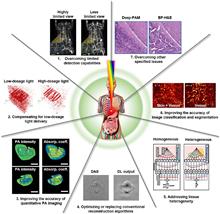
Photoacoustic imaging (PAI), recognized as a promising biomedical imaging modality for preclinical and clinical studies, uniquely combines the advantages of optical and ultrasound imaging. Despite PAI’s great potential to provide valuable biological information, its wide application has been hindered by technical limitations, such as hardware restrictions or lack of the biometric information required for image reconstruction. We first analyze the limitations of PAI and categorize them by seven key challenges: limited detection, low-dosage light delivery, inaccurate quantification, limited numerical reconstruction, tissue heterogeneity, imperfect image segmentation/classification, and others. Then, because deep learning (DL) has increasingly demonstrated its ability to overcome the physical limitations of imaging modalities, we review DL studies from the past five years that address each of the seven challenges in PAI. Finally, we discuss the promise of future research directions in DL-enhanced PAI.
.- Publication Date: Jul. 24, 2023
- Vol. 2, Issue 5, 054001 (2023)
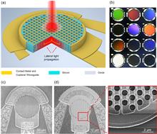
The photosensitivity of silicon is inherently very low in the visible electromagnetic spectrum, and it drops rapidly beyond 800 nm in near-infrared wavelengths. We have experimentally demonstrated a technique utilizing photon-trapping surface structures to show a prodigious improvement of photoabsorption in 1-μm-thin silicon, surpassing the inherent absorption efficiency of gallium arsenide for a broad spectrum. The photon-trapping structures allow the bending of normally incident light by almost 90 deg to transform into laterally propagating modes along the silicon plane. Consequently, the propagation length of light increases, contributing to more than one order of magnitude improvement in absorption efficiency in photodetectors. This high-absorption phenomenon is explained by finite-difference time-domain analysis, where we show an enhanced photon density of states while substantially reducing the optical group velocity of light compared to silicon without photon-trapping structures, leading to significantly enhanced light–matter interactions. Our simulations also predict an enhanced absorption efficiency of photodetectors designed using 30- and 100-nm silicon thin films that are compatible with CMOS electronics. Despite a very thin absorption layer, such photon-trapping structures can enable high-efficiency and high-speed photodetectors needed in ultrafast computer networks, data communication, and imaging systems, with the potential to revolutionize on-chip logic and optoelectronic integration.
.- Publication Date: Jul. 24, 2023
- Vol. 2, Issue 5, 056001 (2023)
- Publication Date: Jul. 22, 2023
- Vol. 2, Issue 5, 056002 (2023)
- Publication Date: Jul. 24, 2023
- Vol. 2, Issue 5, 056003 (2023)

- Publication Date: Jul. 31, 2023
- Vol. 2, Issue 5, 056004 (2023)
- Publication Date: Aug. 01, 2023
- Vol. 2, Issue 5, 056005 (2023)
- Publication Date: Aug. 16, 2023
- Vol. 2, Issue 5, 056006 (2023)
- Publication Date: Sep. 12, 2023
- Vol. 2, Issue 5, 056007 (2023)
- Publication Date: Sep. 13, 2023
- Vol. 2, Issue 5, 056008 (2023)
- Publication Date: Sep. 21, 2023
- Vol. 2, Issue 5, 056009 (2023)
Silicon thermo-optic phase shifters: a review of configurations and optimization strategies
Vol. 3, Issue 4, 044001 (2024)
Flexible depth-of-focus, depth-invariant resolution photoacoustic microscopy with Airy beam
Vol. 3, Issue 4, 046001 (2024)
Highly sensitive mid-infrared upconversion detection based on external-cavity pump enhancement
Vol. 3, Issue 4, 046002 (2024)
Vol. 2, Issue 6, 065001 (2023)
Decision-making and control with diffractive optical networks
Vol. 3, Issue 4, 046003 (2024)
