Inspired by the discovery of graphene, researchers have developed a family of two-dimensional (2D) layered materials and investigated their unique optoelectronic properties. Molybdenum disulfide (MoS2), as a kind of typical 2D material, has been intensively investigated due to potential applications in novel electrical and optoelectronic devices. However, in spite of great efforts dedicated to 2D MoS2 study from both experiment and theory, the main challenge remained to be addressed is to achieve 2D MoS2 with high quality and large area, which is the key point for realization of its commercial application.
Recently, a research group led by Prof. Li from Changchun Institute of Optics, Fine Mechanics and Physics (CIOMP) reported large-area and high-quality single-layer MoS2 grown by chemical vapor deposition (CVD), showing the possibility of breaking the growth challenge by CVD method, which is published on Photonics Research (You Wu, Zhiwen Li, Kah-Wee Ang, Yuping Jia, Zhiming Shi, Zhi Huang, Wenjie Yu, Xiaojuan Sun, Xinke Liu, and Dabing Li, Monolithic integration of MoS2-based visible detectors and GaN-based UV detectors, Volume 7, Issue 10, 2019).
In this work, free-standing GaN wafer was selected as the substrate for 2D MoS2 growth due to lattice-matching between GaN and MoS2. The theoretical and experimental methods were combined to prove the superiority of the GaN substrate, and a large-area and high-quality single-layer MoS2 was obtained.
Based on the successful preparation of 2D MoS2 film, the monolithic integration of high performance visible and ultraviolet dual-wavelength photodetectors is realized by semiconductor fabrication technologies. MoS2 and GaN are responsible for detection in visible and ultraviolet range, respectively. The dual-wavelength photodetector achieved excellent performance in photocurrent gain, external quantum efficiency, and normalized detection rate with low noise equivalent power. The peak photoresponsivity of the GaN-based UV detector is 172.12 A/W, while that of the MoS2-based visible detector is 17.5 A/W. This work provides a feasible solution for integrating multi-color detectors, and the growth methods and device preparation process could also be extended to other 2D material systems, which could broaden the future applications for image sensing and optical communication.
Prof. Li believes that the monolithic integrated dual-color detectors obtained in this work are of great significance for development of high-integration optoelectronic devices. The fabrication method is transplantable to other 2D system, and provides a good reference for the applications of other 2D material systems.
Based on present results, future work of Prof. Li's group will be focused on improvement in growth and device technique for large-area and high-quality 2D materials in order to explore other high-performance multi-color photodetectors.
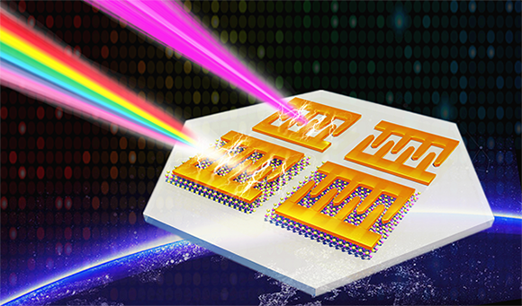

Monolithic integration of MoS2-based visible detectors and GaN-based UV detectors.