At the invitation of the founding editor-in-chief of Photonics Insights, Professor Zhu Jia's team from Nanjing University authored a review paper titled " Plasmon-induced hot carrier dynamics and utilization" which was published in the fourth issue of Photonics Insights, 2024. (Jian Luo, Qile Wu, Lin Zhou, Weixi Lu, Wenxing Yang, Jia Zhu. Plasmon-induced hot carrier dynamics and utilization[J]. Photonics Insights, 2023, 2(4): R08)
This review systematically summarizes the latest advancements in the generation and transport dynamics of hot carriers induced by plasmons and their applications in devices. It focuses on delineating the basic physical picture of plasmon-induced hot electrons, efficient transport and control strategies, and design principles for optimal device performance. Academician Xu Hongxing from Wuhan University, Professor Zhang Shunping, and Yuhao Xu contributed a commentary entitled "Photophysical and photochemical process after light absorption in metals" on this review. They commented highly on the review, saying "The review is timely and comprehensive, delving into a broad spectrum of intriguing topics within the realm of plasmon-induced hot carriers. We posit that this endeavor will significantly facilitate the entry of young researchers into this captivating field".
Plasmons are caused by the collective oscillations of free electrons in conductive materials, capable of compressing electromagnetic fields at the nanoscale and achieving ultimate control of light. For decades, plasmonics has been widely applied in various fields such as photophysics, chemistry, biology, environmental science, and solar energy conversion, becoming one of the most focused subfields in nanophotonics and nanooptics. The coherent charge oscillation at the surface of metal nanoparticles forms surface plasmons. By fabricating metal nanoparticles with adjustable sizes in different environments, it is possible to conveniently design surface plasmons to occur resonance with light of different wavelengths and realize optical modulation.1 The incident electromagnetic waves are confined at the surface of metal nanoparticles, achieving a significant enhancement of the electric field by factors of 104 to 106. This greatly enhances nonlinear optical processes and plays a vital role in many areas, including surface-enhanced Raman spectroscopy, fluorescence sensing enhancement, and the second and third harmonic generation.
The coherent oscillation of surface charges on metal nanoparticles dissipates due to internal damping, leading to the dephasing of surface plasmons. The mechanisms of dephasing are divided into radiative and non-radiative relaxations, closely related to the resonance wavelength, particle size, and the band structure of the metal. Experimentally, methods such as ellipsometry for measuring dielectric functions, single-particle near-field scattering spectroscopy, and femtosecond autocorrelation function measurements can be used to determine the dephasing time of plasmons.
In 2005, Kubo A. et al. first combined the femtosecond interferometric time-resolved techniques with photoelectron emission microscopy, allowing for nanoscale spatial resolution and sub-femtosecond temporal resolution and enabling precise measurement of plasmon dephasing times in different regions of a nanoparticle.2 As shown in Figure 1, the dephasing time of plasmons generally does not exceed 30 femtoseconds and can be as short as within 10 femtoseconds in some cases. In 2020, a research group in Nanjing University first measured the plasmon dephasing time of sodium, which is about two times longer than that of silver. They also fabricated the sodium-based plasmonic nanolaser with an ultralow lasing threshold.3
Non-radiative plasmon dephasing generates high-energy electrons and holes, called as hot electron and holes, respectively. They are collectively known as hot carriers. These hot carriers lose energy through electron-electron and electron-phonon scattering in metals, eventually leading to an increase in the temperature of the nanoparticles. Alternatively, a part of hot electrons reaches the metal-dielectric interface. If they still retaining sufficient energy, they can overcome the interfacial barrier and finally be injected into adjacent semiconductors or molecules, thereby enabling a wider range of applications, such as photocatalysis, photovoltaics, and ultrafast optical modulation.
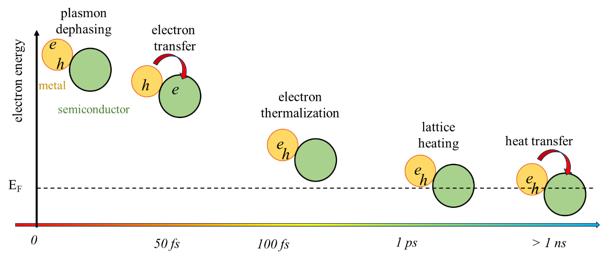
Figure 1. Schematic representation of the time scale for the evolution of plasmon-induced hot carriers.
The generation of hot electrons through non-radiative dephasing of plasmons is a result of the interaction between light and electrons, obeying both energy conservation and momentum conservation. As illustrated in Figure 2, for noble metals like gold and silver, non-radiative dephasing mechanisms include interband transition mechanism and three types of intraband transition mechanisms: electron-electron scattering; phonon-assisted intraband transitions and surface damping (also known as Landau damping). In the mechanism of interband transitions, most of the photon energy contributes to the energy gap between the d-band and the Fermi level, thus the kinetic energy transferred to the electrons is minimal. These electrons are not "hot" enough to overcome the metal-dielectric interfacial energy and are confined within the metal.
Therefore, interband transitions should be avoided in applications based on hot carrier transfer. Unfortunately, when the resonance energy of plasmons exceeds the bandgap, interband transitions dominate the mechanism of hot electron generation. Intraband transitions due to electron-electron scattering produce two electrons, each with half the energy of the absorbed photon, known as "warm" electrons. Phonon-assisted intraband transitions use phonons to compensate for the required momentum. Since phonons have much lower mass than electrons, the electron absorbs most of the photon energy, becoming a "hot" electron. Similarly, surface damping compensates for momentum through the surface, also generating "hot" electrons.
However, the proportion of hot electrons generated by surface damping moving towards the surface is higher than that of phonon-assisted hot electrons, offering a greater chance of crossing the metal-dielectric interface. Therefore, to increase the efficiency of hot electron production, it is necessary to enhance the proportion of the surface damping mechanism. Alternatively, narrowing the depth of the sp-band and exciting the same plasmon continuously by two pulses (Figure 2) are also able to promote hot electron generation. For non-noble transition metals (such as Fe, Co, Ni) and main group metals (such as Al), their band structures differ from noble metals, and interband transitions can also produce hot electrons. However, their stabilities are far from noble metals, impeding their application as plasmonic metals.
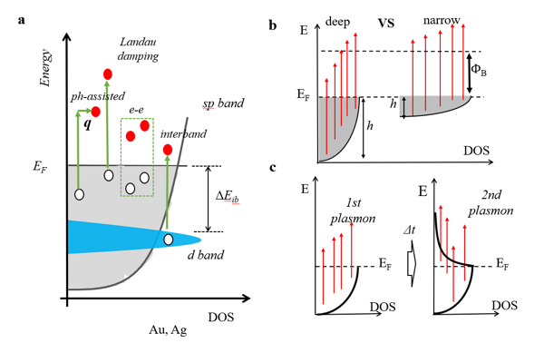
Figure 2. (a) Schematic illustration of four mechanisms for hot electron generation in noble metals (Au, Ag). (b) Promotion of hot electron generation by reducing the depth of the sp-band. (c) Enhancement of hot electron generation through continuous excitation of the same plasmon.
Plasmon-induced electron transfer can be categorized into two mechanisms: direct and indirect electron transfer. As shown in Figure 3, in the direct electron transfer mechanism, electron transfer occurs simultaneously with the dephasing of plasmons, thus direct electron transfer is a type of surface damping.4 In the indirect electron transfer mechanism, electrons are first generated inside the metal and then transported toward the interface, finally injected to the adjacent dielectrics. In the transportation, hot electrons will lose energy due to electron-electron and electron-phonon scatterings and generate photothermal effect.5 Thus, the injection efficiency is lowered significantly.
The transportation process is avoided in the direct electron transfer mechanism, making the electron injection efficiency much higher than the efficiency in indirect electron transfer mechanism. However, the hot electrons generated on the conduction band of adjacent dielectrics by direct electron transfer possess strong interfacial characteristics and are confined near the interface,6 making them more easily to recombine with the holes in metal at the interface and thus more difficult to diffuse into the interior of dielectrics compared to hot electrons injected by indirect transfer, thereby reducing the extraction efficiency of hot electrons.
Overall, although the direct electron transfer mechanism exhibits higher electron injection efficiency than the indirect mechanism, the efficiency of ultimate electron extraction and utilization does not show a significant difference between them. Therefore, it is necessary to design the metal-dielectric interface to promote hot electrons away from the interface, such as designing semiconductor structures to support fast electron diffusion, using piezoelectric materials to alter the interfacial electric field (Figure 3) and applying external bias. The electron-hole recombination is thus inhibited and the overall electron utilization efficiency is improved.
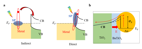
Figure 3. (a) Schematic diagram of indirect and direct electron transfer mechanisms. (b) Illustration of how piezoelectric materials alter the interfacial electric field to promote electron diffusion.
So far, the utilization efficiency of hot carriers induced by plasmons is not high due to many factors such as the low generation efficiency of hot carriers, energy loss during transportation, and electron-hole recombination at the interface. However, as the understanding of hot carrier generation mechanism deepens and efficient methods of interfacial structure modulation develops, it will inevitably lead to improved utilization efficiency of hot carriers. Plasmon-induced hot carrier transfer opens an avenue to surface photocatalysis.7 Combining the plasmonic hot spots with the catalytically active sites largely increases the photocatalytic efficiency (Figure 4).8 Moreover, plasmon-induced hot carriers have shown promising prospects in areas such as photovoltaics, photoelectric detection, and ultrafast optical modulation. The incident photo-current efficiency can be improved significantly by adding transport layer. A combination of plasmonic metals and semiconductors achieves high-sensitive photodetection on UV light. Moreover, the femtosecond all-optical modulation is achieved benefiting from the ultrafast transport of hot carriers from metals to semiconductors(Figure 4).
Figure 4. Applications of plasmon-induced hot carriers in (a) photocatalysis, (b) photovoltaics, (c) photoelectric detection, and (d) ultrafast optical modulation.
The Professor Zhu group has reviewed the dynamics and utilization of hot carriers induced by plasmons, including the nature and measurement of plasmon dephasing, the generation mechanisms of hot carriers and methods to enhance their generation efficiency, mechanisms of electron transfer, methods to improve electron utilization, and applications of hot carriers. This review constructs a fundamental physical picture from the generation to the extraction of hot carriers, providing comprehensive understanding and new insights for researchers in the field. In the future, development of experimental techniques with high spatiotemporal resolution and more accurate solid theory will give more insight into the nature of plasmons and promote to find a way to improve the hot carrier generation efficiency. In addition, developing novel materials supporting fast hot carrier transport and long hot carrier lifetime will greatly improve the hot carrier utilization efficiency. As a result, devices based on plasmon-induced hot carriers will not only provide a solution for the energy crisis by efficiently utilizing solar energy but also play an important role in information science benefitting from its femtosecond all-optical modulation.