Two-dimensional (2D) materials with only single to several atomic layers, exhibit surprisingly strong light-matter interactions, for example, the exitonic absorption in monolayer transition metal dichalcogenides (TMDCs) can be as large as 20%. There are many kinds of 2D materials with diverse band structures and high tunability, exhibiting rich optical properties.
In low symmetry 2D materials, in-plane anisotropic crystal structure not only induces well-known phenomena such as linear dichroism in absorption, birefringence and so on, but also renders additional freedom to control and detect light. In certain cases, the anisotropy gives rise to different optical conductivities along different main axis, forming hyperbolic polaritons. These special polaritons with extremely large photonic density of states and directional propagating rays are very fascinating in photonics. All of these indicate much richer light-matter interactions in low symmetry 2D materials.
The study on low symmetry 2D materials originates from the emergence of 2D black phosphorus in 2014. Up to now, decades of anisotropic 2D materials have been discovered. According to the crystal structure, anisotropic 2D materials can be divided into orthorhombic systems [e.g., BP, black arsenic (B-As), group IV monochalcogenides MX (M = Ge, Sn; X = S, Se), etc.], monoclinic systems (e.g., 1T' WTe2, TiS3, etc.), and triclinic systems (e.g., ReX2, X = S, Se).
Here, a team of scientists led by Prof. Yan at Fudan University was invited by Co-Editors-in-Chief to contribute a comprehensive review paper entitled "Optical properties and polaritons of low symmetry 2D materials", which was published in the Volume 2, Issue 1 of Photonics Insights. In this paper, fundamental optical properties and polaritons of various anisotropic 2D materials have been reviewed, especially for the anisotropic interband absorption, photoluminescence, exciton, non-linear optics and various types of hyperbolic polaritons. Lastly, conclusions and perspectives for future research are given.
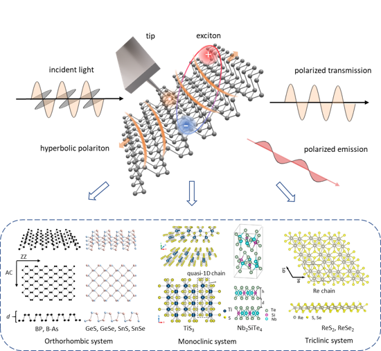
Figure 1. Optical properties and polaritons of low symmetry 2D materials
1 Optical properties of low-symmetry 2D materials
1.1 Interband absorption and photoluminescence
Most optoelectronic devices work in the IR to visible regime, where the interband transition plays a critical role in light absorption, termed as interband absorption. Through Fermi's golden rule, the interband absorption is proportional to the joint density of states and interband transition probability, and the latter is closely related to band structure. Due to the layer-dependence and anisotropy in low symmetry 2D materials, the main characteristics of interband absorption are the layer-dependence and anisotropy. For example, in black phosphorus interband absorption energy changes from mid-infrared to visible regime when the thickness decreases from bulk to monolayer. And interband absorption is forbidden when incident light is polarized along the zigzag direction. Similar scenarios can be found as well in other low symmetry 2D materials (Fig. 2).
The converse process of interband absorption is interband photoluminescence (PL), which shares the same polarization dependence with interband absorption. In contrast, PL is sensitive to defect states, which could give rise to the Stokes shift. Besides, defects can also change the polarization dependence of PL, such as in TiS3 the polarization dependence of defect states PL is just opposite to that of the interband PL. Hence, PL properties can be artificially manipulated by defect engineering.

Figure 2. Interband absorption of low symmetry 2D materials
1.2 Exciton
Due to the enhanced quantum confinement and reduced dielectric screening in 2D materials, the excited electrons and holes can be tightly bounded by Coulomb interactions, which is termed as exciton. In anisotropic 2D materials, excitonic absorption and PL inherits the polarization dependence of the interband transition. Besides, exciton wave functions possess anisotropy as well, e.g., the wave functions of bright excitons in monolayer BP are more extended along the armchair direction to form striped patterns, similar to those in nanowires.
Recently, hybrid dimension excitons have been reported, such as those in 2D SiP2, where the electrons constituting the excitons are confined within 1D phosphorus–phosphorus chains, while the holes are extended over the 2D SiP2 plane. This unique exciton exhibits strong exciton-phonon coupling. Overall, studies in anisotropic 2D materials will further enrich excitonic physics (Fig. 3).

Figure 3. Excitons in low symmetry 2D materials
1.3 Tuning of optical properties
Optical properties of anisotropic 2D materials can be efficiently tuned by various methods (such as electrical field, strain, pressure, doping, intercalation and so on). For example, in few-layer BP, the PL wavelength can change from 5.5 um to 3.2 um with moderate strain changing from -0.66% to 1.21%. Under enough electrical field, BP can be converted from a semiconductor to an anisotropic Dirac semimetal.
Furthermore, in-plane anisotropy also renders a new freedom to the band structure engineering. Especially for the van der Waals hetero/homo structure, in-plane anisotropy could introduce unique properties. For example, in homo/heterostructures based on graphene or TMDCs with hexagonal structure, the prominent moiré effect can be observed only within a tiny interlayer twisted angle (<2°), while a strong moiré effect persists even at a large angle of ∼19° in mono- and bilayer BP homostructures.
Figure 4. Tuning of optical properties
2 Polaritons of low-symmetry 2D materials
2.1 Methods for probe of polaritons
Unlike other optical measurements (e.g. absorption, PL…), direct illumination of light from free space on materials is unable to excite polaritons due to the momentum mismatch of photons and polaritons. Thus, methods are required to compensate the momentum mismatch for the probe of polaritons, including both near- and far-field techniques. Far-field techniques usually detect the reflection, transmission, absorption or scattering of the specimen at macroscopic scale with the aid of a prism with high refractive index or fabricated gratings to excite polaritons (Figs. 5a and 5b).
The near-field techniques include the scattering-type scanning near-field optical microscopy (s-SNOM) and the electron energy loss spectroscopy based on scanning transmission electron microscope (STEM), which can probe spatially resolved properties of polaritons beyond the diffraction limit. In comparison, Near-filed techniques have higher space resolution, while the far-field techniques can cover a wider spectral range.
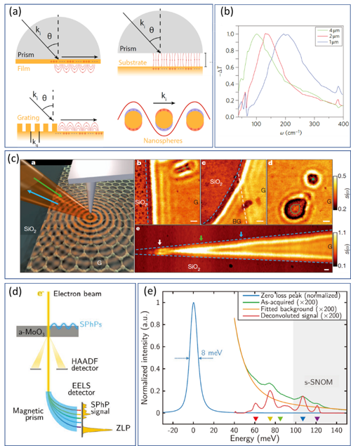
Figure 5. Methods to probe polaritons.
2.2 Hyperbolic polaritons
- Natural hyperbolic phonon polaritons
Hyperbolic polaritons can be realized in natural 2D surface in the spectral range with a sign-changing in-plane conductivity/permittivity. Such conditions can be maintained in 2D surfaces with anisotropic phonon excitations. The first natural in-plane hyperbolic phonon polaritons were observed in -MoO3, which possesses anisotropic optical phonons between 820 and 1010 cm-1.
Evidence of hyperbolic phonon polaritons in MoO3 was firstly reported in 2018 by s-SNOM experiments (Figure 6(a)-(d)). High filed confinement and long lifetime are discovered. Other methods, such as EELS, are also adopted to investigate the hyperbolic phonon polaritons (Figs. 6(e) and (f)). Subsequently, more 2D materials with in-plane anisotropic phonons have been discovered to support natural hyperbolic phonon polaritons, such as -V2O5, -GeS, which extend the spectral range of natural hyperbolic polaritons to THz range.

Figure 6. In-plane hyperbolic phonon polaritons in α-MoO3
- Natural hyperbolic plasmon polaritons
The experimental realization of hyperbolic plasmon polaritons was first observed in WTe2 single crystal films in 2020. The hyperbolic plasmons were observed at 10 K, with spectral range of 16 μm to 23 μm. By the far-field method, anisotropic plasmon dispersion was resolved by probing resonance peaks in different ribbon/disk arrays of WTe2 films (Fig. 7(h). The topological transition from elliptic to hyperbolic regime of plasmon iso-frequency contours was successfully mapped (Fig. 7(i)). In contrast to phonon polaritons, hyperbolic plasmon in 2D materials are formed by the cooperation of anisotropic intraband and interband electronic transitions (Figs. 7 (d) and (f)).
More importantly, WTe2 is a well-studied topological material, called type II Weyl semimetal, which possesses many distinct electronic properties, such as extremely high mobility, temperature-dependent band structures, quantum spin hall insulator and gate-induced superconductivity in monolayer. All these properties establish WTe2 as a suitable platform for exploring new intriguing properties of hyperbolic plasmons.
In theory, many other materials have been proposed to sustain hyperbolic plasmons, such as BP, in a wide range from terahertz to visible frequencies. Other candidates include cuprates, monolayer MoOCl2 and NaW2O2Br6, carbon doped monolayer phosphorene (β-allotrope of carbon phosphide). Tunable hyperbolic regime is predicted in these materials by strain, chemical or electrostatic doping.
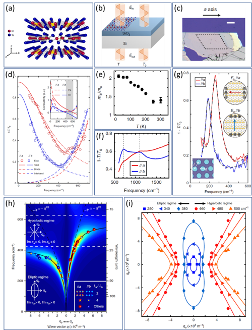
Figure 7. In-plane hyperbolic plasmon polaritons in WTe2
- Natural hyperbolic exciton polaritons
Excitons can also couple to free space photons, which leads to propagating exciton polaritons confined to 2D surfaces. Similar to phonon and plasmon polaritons, a sign-changing in-plane conductivity is needed to support the hyperbolic dispersion of exciton polaritons. Possible candidates are 2D materials with anisotropic exciton excitations, e.g., BP, which has highly anisotropic excitons from MIR to visible wavelength depending on the thickness.
In 2021, successful measurement of highly anisotropic reflection spectra was realized in monolayer BP (Fig. 8 (a)) with a sharp and strong 1s exciton resonance with polarization along AC direction (Fig. 8(b)). Based on the results, the sheet optical conductivity for the monolayer BP can be extracted, demonstrating a sign-changing regime sustaining the hyperbolic exciton polaritons (Fig. 8(c)). The exciton resonance frequency redshifts as the layer number increases from 1L to 4L (Fig. 8(e)), and consequently, the hyperbolic regime moves to lower frequencies (Fig. 8(f). In fact, many other methods can be used to tailor the exciton frequency of BP films in the future, such as strain, temperature, pressure, electric gating and intercalation.
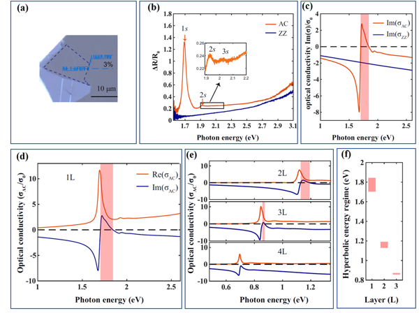
Figure 8. In-plane hyperbolic exciton polaritons in few layer BP films
2.3 Methods for polariton engineering in Anisotropic 2D Surfaces
How to tailor polaritons is the most important question after the discovery of hyperbolic polaritons. By changing the anisotropy of the 2D surfaces or the dielectric environment, one expects to modify the permittivity anisotropy, the iso-frequency contours of polaritons and even hyperbolic spectral range, which will exhibit much potential for applications requiring specific control of polariton propagation, for example, coupling between quantum emitters or heat management.
Many methods have been reported in tuning the hyperbolic polaritons, especially for hyperbolic phonon polaritons. One scheme is to design heterostructures, such as fabricating twisted bilayer structures or graphene/2D films heterostructures. Polaritons in two layers can couple with each other through evanescent waves, which gives rise to modifications to the propagation of polaritons.
The propagation direction and the shape of the plasmon mode can be tailored by changing the twist angle (Fig. 9(a)) or doping graphene (Fig. 9(b)). The second method is to change the substrates. One can choose a suitable substrate, such as polar substrates or phase change materials, to have the desired dielectric permittivity values or signs to control the polaritons on the anisotropic 2D surface. For example, unidirectional and steerable excitations of polaritons have been achieved by placing α-MoO3 films on polar dielectric cavities ((Fig. 9(c)). The third method is to change the properties of lattice vibrations intrinsically by intercalating other atoms into the polar vdWs crystal. One example is polaritons in α-V2O5, the reststrahlung band of which can be changed by intercalating Na atoms (Fig. 9(d)).
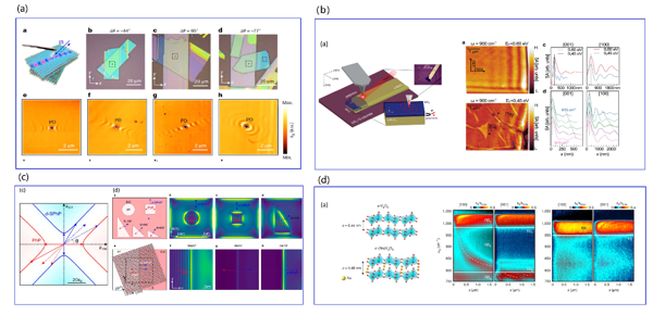
Figure 9. Methods for polariton engineering in Anisotropic 2D Surfaces
2.4 Applications of Polaritons in Hyperbolic 2D Surfaces
The discovery of natural anisotropic vdWs surfaces introduces an ideal platform for exploiting the effect of in-plane anisotropy in the application of planar optical devices. Especially in the hyperbolic regime, polaritons host open IFCs, theoretically infinite wave vectors, directional propagation, and extremely large optical DOSs, exhibiting great potential for nano-confinement of light, polarization engineering, and enhancement of light–matter interactions. In addition, most of the discovered natural hyperbolic 2D surfaces are in the MIR and FIR spectral ranges, which is of immense importance for applications in various fields, such as astronomy, medical diagnosis, sensing, and imaging. The vdWs nature makes it easier for miniaturization and integration of IR optical components.
One application is polarization engineering based on the extreme optical properties in natural hyperbolic materials, such as wave plate, circular dichroism and asymmetric transmission. It is noted that such polarization engineering is achieved on natural surfaces without using complex lithography. The device can be further tuned based on the tailoring methods discussed above.
The second application is the polariton propagation manipulation, which is essential for constructing compact planar nanophotonic devices and circuits. Such manipulation was previously realized on metamaterials or metasurfaces which were limited by the size and loss of artificial optical structures. The distinct dispersion of naturally hyperbolic materials opens up a new avenue to manipulate light and energy flow. Many applications have been reported such as polariton nanofocusing, field canalization, negative reflection and unidirectional propagation of polaritons.
The third application is the enhancement of spontaneous emission (SE), which has important effects on the development of biomedical sensing and nanophotonics. The discovery of natural hyperbolic polaritons on 2D surfaces has provided a new platform to study the SE enhancement, since they avoid complicated nanofabrication and host even higher optical DOSs and stronger field confinement. For example, the order of magnitude of the SE enhancement rate has been predicted to exceed 1000 in the natural hyperbolic range. Such tunable anisotropic SE enhancement can be applied to spontaneous valley coherence, which is important for realizing applications of quantum technologies.
The last application is management and modulation of thermal radiation and heat transfer. In fact, the thermal transfer can also be realized by the evanescent waves near the surface, which surpasses blackbody radiation, opening routes for applications such as noncontact thermal management and modulation, subwavelength thermal imaging, and efficient enhancement of radiative cooling and waste heat recovery. Naturally hyperbolic 2D materials provide a distinct platform for controlling near-field thermal radiation due to their theoretically infinite optical DOSs and easy implementation for planar photonics. For example, the near-field radiative heat flux (RHF) can be enhanced in the two suspended sheet systems over 102 to 104 times that for the blackbody limit due to the presence of anisotropic and hyperbolic plasmon polaritons.
3 Summary and outlook
Prof. Yan group thoroughly reviewed research progress in optical properties and polaritons of low symmetry 2D materials. Furthermore, they proposed some promising research directions in the future, such as: exploring emerging anisotropic atomically thin materials, homo/heterostructures based on anisotropic 2D materials, integrating anisotropic 2D materials with photonic systems, exploring new types of hyperbolic polaritons, active tuning schemes for hyperbolic polaritons, exploring hyperbolic polaritons in strongly correlated and topological materials and so on.