Nanophotonic devices, which take photons as information carries, play key roles in next-generation photonic chip. The design of multifunctional and practical devices has always been one of the core topics of nanophotonic devices. However, traditional design methods rely on human experience and physical inspiration for structural design and parameter optimization, so they often consume a lot of computing resources to obtain excellent results, and the structure type is not abundant enough.
In recent years, the application of intelligent algorithms in the field of nanophotonic devices develops rapidly. It is universal and efficient in designing nanophotonic devices with different materials, different structures, different modes and different wavelengths. Using intelligent algorithms to design nanophotonic devices can break the limit of traditional methods and predict new structures. Therefore, intelligent algorithms provide new avenues in designing nanophotonic devices.
Intelligent algorithms are practical alternative techniques for solving varieties of challenging engineering problems, which are methods inspired by natural phenomena or laws. People use intelligent algorithms to solve practical problems by learning or imitating natural principles. In many practical applications, intelligent algorithms are used to deal with various challenging problems. Whether it is an intricate continuous problem or a discrete problem to be optimized, intelligent algorithms can be applied under both cases and find feasible solutions in a short time.
It shows that the avenues of designing nanophotonic devices based on intelligent algorithms will be an important direction for the future development of nanophotonics. Intelligent algorithms are important core techniques for parameter tuning and computer-aided design of devices, which can establish a clear and intuitive physical scene for the devices working principle. The design efficiency can be greatly improved by using the appropriate algorithm, and the best performance of the device can be expected. Therefore, the study of intelligent algorithms is of great practical significance to the design of nanophotonic devices.
Recently, Prof. Cuicui Lu et al. from Beijing Institute of Technology are invited to review the intelligent algorithms for designing nanophotonic devices from the design principle and applications. They expect to give a comprehensive summary for the applications of intelligent algorithms in designing nanophotonic devices. The research results are published in Chinese Optics Letters, Vol. 19, No. 1, 2021 (Lifeng Ma, Jing Li, Zhouhui Liu, Yuxuan Zhang, Nianen Zhang, Shuqiao Zheng, Cuicui Lu. Intelligent algorithms: new avenues for designing nanophotonic devices [Invited] [J]. Chinese Optics Letters, 2021, 19(1): 011301).
One of the group members Zhouhui Liu said "in the recent two years, we have realized the smallest on-chip wavelength router and polarization routers by using the finite element method and genetic algorithm. We now try to combine more optimization algorithms together, such as simulated annealing algorithm, topology optimization, and more efficient multi-functional nanophotonic devices are expected to be realized."
Summary of intelligent algorithms and their applications for designing nanophotonic devices
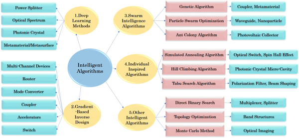
In this review, a variety of intelligent algorithms are discussed in detail. The deep learning methods, the gradient-based inverse design method, swarm intelligence algorithms [including genetic algorithm (GA), particle swarm optimization (PSO) and ant colony algorithm (ACA)], individual inspired algorithms [including the simulated annealing algorithm (SAA), the hill climbing algorithm and tabu search (TS)] and some other algorithms [including the direct binary search (DBS) algorithm, topology optimization, and Monte Carlo method] are introduced from the research background or concept to the applications for designing nanophotonic devices. Some representative application examples of nanophotonic devices are listed under each mentioned intelligent algorithm. The intelligent algorithms and their applications for designing nanophotonic devices are summarized and analyzed.
Compared with the traditional design methods, the intelligent algorithms are universal and efficient. For example, the advantage of deep learning is that after training, it has less computational cost and is more likely to find better optimal solutions than traditional algorithms. In addition, compared with traditional algorithms, the deep learning methods can realize inverse design more easily. ANN has many typical structures and strong flexibility. According to the design requirements in the training process, we can choose the appropriate neural network for optimal design.
The gradient-based inverse design method can automatically design nanophotonic devices and only require the user to input high level parameters. This method can provide large parameter space and design devices using full space parameters of manufacturable devices, which often requires less simulation than GA or PSO because they do not rely on parametric scanning or random perturbations to find the minima. This method can be used to design any passive, linear photonic device. However, the implemented design usually presents a continuous terrain, and some tiny structural components may be formed during the inverse design process, which presents a challenge to sample making.
Swarm intelligence algorithms have certain robustness and strong evolutionary or search ability. For instance, GA can not only solve single-objective optimization problem, but also plays a greater role in multi-objective optimization problems. It has the characteristics of group search and is suitable for solving complex optimization problems, such as the need to optimize multiple system parameters at the same time. Moreover, GA is scalable and easy to be combined with other algorithms. The researchers also introduced some other intelligent algorithms, such as individual inspired algorithms, which can give a better solution in a certain acceptable time, but cannot be guaranteed to be optimal.
All intelligent algorithms have their own advantages and disadvantages, and this review explains the developing trend of using intelligent algorithms through the analysis and summary of the principles and applications of intelligent algorithms, especially in the future design of nanophotonic devices. As the need for nanophotonic devices to achieve more functions is further strengthened, the intelligent algorithms, especially the more popular method (e.g., deep learning methods) with higher efficiency and better effect, will continue playing a significant role in the design of nanophotonic devices to implement complex functions and improve the performance of nanophotonic devices. This will provide an avenue for the realization of photonic chips in the future.
As for the utilization of intelligent algorithms, multiple algorithms can be adopted simultaneously to provide efficient and optimal solutions during the design process of nanophotonic devices, rather than just one algorithm. In addition, when too many algorithms are difficult to choose, the more reports some algorithms appear in, the more frequently they have been used, which may be a reference for similar problems.