An optical waveguide structure is characterized by a region with relatively high refractive index surrounded by regions with lower index. Benefiting from their compact size, optical waveguides have been considered to be one of the key building blocks for on-chip photonic circuits. As passive devices, waveguides can be used as optical switcher, splitter, multiplexer and coupler and so on. Furthermore, many of the optical effects in the substrate materials can be realized in optical waveguides. Due to the high intra-cavity light energy, many performances could be considerably enhanced in the wave-guiding structures, such as low threshold for waveguide lasers, fast responses for frequency conversion in nonlinear waveguides, which is a promising feature for the practical applications of waveguide devices as well as integrated optical circuits.
Femtosecond laser inscription (FLI) has been recognized as an efficient tool to fabricate waveguides in versatile crystals owing to the powerful 3D engineering capability and micro-scale localized refractive index modification. Generally, discrete inscription approach is used to fabricate cladding waveguides by multiple writing of a number of parallel tracks around a defined contour with circular, rectangular or rhombic shapes. Furthermore, the cladding configurations can also be achieved by applying the helical inscription scheme, i.e., the material is translated along a helical trajectory during the FLI process. Under this condition, the cladding is formed within a single helical inscription process and delivers a continuous and smooth aspect of the cross sections.
The research group led by Prof. Yangjian Cai from Shandong Normal University fabricate cladding waveguides in Pr:YLF by femtosecond laser helical inscription. With the optimized parameters, low propagation loss of the waveguide is achieved. Efficient waveguide lasers in orange are realized with low lasing threshold and enhanced slope efficiency. The research results are published in Chinese Optics Letters , Volume 20, No. 12, 2022(Yingying Ren, et al. Laser emission from low-loss cladding waveguides in Pr:YLF by femtosecond laser helical inscription).
In this work, several cladding waveguides in Pr:YLF crystal are fabricated by femtosecond laser helical inscription, as shown in Figure 1. The cross-section of the cladding waveguides show elliptical geometries which are are deeply embedded inside the sample without any evident damage either in the core areas or in the bulk outside the claddings, highlighting the unique capability of FLI for internal micro-fabrication. All waveguides show strong optical confinement under both 633 nm and 1604 nm. Polarization analyses of the waveguides are performed by measuring all-angle output power by using an end-coupling system, indicating slight polarization sensitivity of the waveguides. Low propagation losses around 0.12 dB/cm is achieved when the optimized parameters (300 nJ pulse energy and 50 μm/s scanning speed) are used for waveguide fabrication. For comparison, similar structures are realized by classical translation of the medium. It is revealed that waveguides fabricated by femtosecond laser helical inscription have lower propagation losses when compared with structures realized by classical discrete inscription approach. Further investigations on the confocal mappings of Pr3+ luminescence are performed to get complete knowledge on the spatial variation of the emission line at 641nm and further on the spatial distribution of the micro-structural changes. Results (Figure 2) shows a high density of lattice defects and imperfections in cladding area, while the μ-PL spectral properties are almost unchanged inside the guiding core, making the waveguide even promising for laser generation.
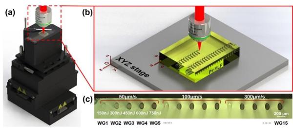
Figure 1. (a) Schematic illustration of the XYZ translation stage for waveguide fabrication using femtosecond laser helical inscription. (b) Schematic of fabrication process. (c) The microscopic photographs of waveguide cross-sections. The fabrication parameters are shown in (c).
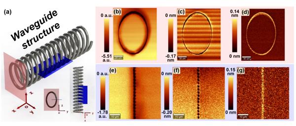
Figure 2. (a) Schematic showing of a waveguide structure and the areas for 2D µ-PL mappings. Spatial dependence of the intensity ((b) and (e)), energy shift ((c) and (f)) and the change in FWHM ((d) and (g)) of the 641 nm emission line obtained from a wide area covering waveguide cross-section and several sections of the loops, as indicated with the planes in red and blue in (a), respectively.
Π-polarized 604 nm waveguide lasers are realized under InGaN-LD excitation at 444 nm, as shown in Figure 3. Based on the most optimized waveguide structure, a highest output power of 120.6 mW is achieved with pumping threshold of 119.8 mW and slope efficiency of 16.6%. Compared with the previous work on Pr:YLF bulky lasers, our waveguide laser systems, although do not have as high performance, show prominent merits in terms of highly compact lasing oscillation cavity and low threshold pump power of 604 nm radiation. Further comparison with the previously demonstrated Pr:YLF cladding waveguide lasers show that the ones produced here are more advantageous as integrated laser devices for reduced pumping thresholds and enhanced efficiencies.
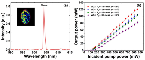
Figure 3. (a) Optical spectrum of waveguide laser centered at 604 nm. The inset shows the normalized spatial intensity distribution of the output laser mode. (b) Output laser power of the waveguides as a function of incident pump power.
"This is the first realization, to the best of our knowledge, of cladding waveguides in Pr:YLF crystal by using femtosecond laser helical inscription. The waveguides laser systems possess superior properties in terms of high compactness, low lasing threshold and enhanced efficiencies. Benefiting from their optimized performances, the waveguides produced in this work are promising for applications as compact orange laser sources. Furthermore, concerning the flexibility and capability of the helical inscription in the structural view, it is believed that more complex structures such as waveguide splitters and near-surface waveguides sensors can be fabricated by specially designing the processing trajectories," says Prof. Yangjian Cai.