Author Affiliations
1State Key Laboratory for Modern Optical Instrumentation, Center for Optical & Electromagnetic Research, College of Optical Science and Engineering, International Research Center for Advanced Photonics, Zhejiang University, Hangzhou 310058, China2Ningbo Research Institute, Zhejiang University, Ningbo 315100, China3Department of Physics, Indian Institute of Technology Roorkee, Roorkee-247 667 Uttarakhand, India4Centro de Tecnologia da Informação Renato Archer-CTI, Rodovia Dom Pedro I, km 143,6, Campinas 13069-901, São Paulo, Brazil5e-mail: yiweixie@zju.edu.cn6e-mail: dxdai@zju.edu.cnshow less
Abstract
A novel wavelength-selective optical switch based on a (GST)-assisted microring-resonator (MRR) is proposed. The present GST-assisted MRR consists of two access optical waveguides and an MRR coupled with a bent GST-loaded silicon photonic waveguide. The optical switch is switched ON or OFF by modifying the GST state to be crystalline or amorphous. In particular, the microring waveguide and the bent GST-loaded waveguide are designed to satisfy the phase-matching condition when the GST is crystalline. As a result, the MRR becomes highly lossy and the resonance peak is depressed significantly. On the other hand, when it is off, there is little coupling due to the significant phase mismatching. Consequently, one has a low-loss transmission at the drop port for the resonance wavelength. In this paper, the simulation using the three-dimensional finite-difference method shows that the extinction ratio of the designed photonic switch is at the resonance wavelength, while the excess losses at the through port and drop port are 0.9 dB and 2 dB. In particular, the resonance wavelength changes little between the ON and OFF states, which makes it suitable for multichannel wavelength-division-multiplexing systems.1. INTRODUCTION
Optical interconnect has been developed successfully as a newly rising technology to overcome the bottlenecks of link capacity and power consumption in traditional electrical interconnects [1,2]. In order to realize reconfigurable photonic networks/systems, an optical switch is an indispensable building block to enable all-optical signal routing and switching. It is desired to develop high-performance optical switches with low excess losses, high extinction ratios, and low power consumption to satisfy the system demands. As is well known, silicon photonics has attracted intensive attention as a very promising platform for realizing photonic integrated devices and circuits because of its unique advantages, such as the high integration density and the complementary-metal-oxide-semiconductor (CMOS) compatibility [3]. Great progress has been achieved on the basic silicon photonic switches [4] and the array [5,6].
For the realization of silicon photonic switches, there are two popular structures. One is utilizing the two-beam interference occurring in a Mach–Zehnder interferometer (MZI), and the other is utilizing the resonance happening in a microring resonator (MRR). For most of these silicon photonic switches, the needed phase-delay variation is introduced thermally or electrically by a phase-shifter using the thermo-optic (TO) effect [7,8] or carrier-induced electro-optical (EO) effects [9,10]. Note that the modulation of the refractive index from the TO or EO effects in silicon is not strong, and the index change is usually on the order of 0.001–0.01. Thus, MZI-based optical switches usually have a large footprint (hundreds of micrometers). In contrast, MRR-based optical switches have compact footprints and can be used for realizing wavelength-selective optical switching in wavelength-division-multiplexing (WDM) systems. For traditional MRR-based optical switches, a given wavelength channel can be switched to the drop port or through port by shifting the resonance wavelength. On the other hand, this wavelength-shift approach is limited in order to avoid the crosstalk from the adjacent channels in a multichannel WDM system. As a result, the MRR should have a very narrow 3 dB bandwidth to guarantee a sufficiently high extinction ratio, even when the wavelength shift is small [11]. Therefore, MRR-based optical switches usually have very limited working bandwidth, and one must control the resonance wavelength carefully. Furthermore, these switches based on the TO or EO effects are volatile, and continuous supply of power is required to maintain their switching state. This prevents to achieve low power consumption.
Recently, phase-change materials (PCMs) have been recognized as a promising candidate for reconfigurable photonic devices due to their nonvolatility [12,13]. In particular, (GST) [14], which has a drastic change in electrical and optical properties when transiting between the amorphous and crystalline states, has shown great potential advantages. Currently GST has been applied widely in different fields including optical switching and routing [14–22], modulation [23,24], multilevel storage [25], and neural computing [26]. The complex refractive index (including the real and imaginary parts) of GST has significant variation when it changes between the amorphous and the crystalline states, which introduces huge phase and amplitude modulations within a compact device footprint. This is very attractive for realizing photonic switches. In addition, the nonvolatility of GST implies that power consumption is required only during the phase transition process and no power is consumed to maintain the state. The phase transition, which is determined by the glass transition temperature and the melting temperature, can be induced electrically, thermally, or optically. The transition speed could be as fast as nanoseconds [27]. Currently, some MRR-based optical switches with GST were proposed by introducing a GST thin layer on a small part of the microring waveguide [15–17]. In Ref. [15], a wavelength-selective optical switch based on a regular GST-assisted all-pass MRR was demonstrated with an extinction ratio of 12.5 dB and an excess loss of 2.5 dB for light transmission at the through port. For this kind of MRR optical switch, it is possible to improve the extinction ratio and reduce the excess loss by utilizing the critical coupling and resonance wavelength shift as demonstrated more recently [16]. On the other hand, it is really desired to realize a high-performance optical switch, which is the building block for reconfigurable optical systems. Unfortunately, it is very challenging to realize optical switches with low losses and high extinction ratios by using a regular GST-assisted MRR. For example, for the wavelength-selective optical switch realized with a regular GST-assisted add-drop MRR [17], the excess losses for the through ports and drop ports are 4.3 dB and 5.1 dB, respectively, while the extinction ratios are about 5.7 dB. It can be seen that the GST layer inserted in this MRR introduces a high loss and lowers the extinction ratio even in theory.
Sign up for Photonics Research TOC. Get the latest issue of Photonics Research delivered right to you!Sign up now
In this paper, we propose a novel nonvolatile MRR-based optical switch, which consists of two access optical waveguides and a microring resonator coupled with a bent GST-loaded silicon photonic waveguide. Here the microring waveguide and the bent GST-loaded silicon photonic waveguide are designed optimally so that the phase-matching condition is satisfied between them when the GST is in the crystal phase. In this case, high power is coupled out from the microring waveguide, which results in a high overall loss for the MRR. Thus, the resonance peak at the drop port is depressed significantly, and correspondingly one has a low-loss transmission at the through port for the resonance wavelength. On the other hand, when the GST transits to the amorphous phase, the significant optical phase mismatch between the microring waveguide and the bent GST-loaded silicon photonic waveguide becomes significant, and thus the coupling between them is reduced. Consequently, a low-loss transmission at the drop port for the resonance wavelength is achieved. In particular, when the device is switched ON or OFF, the resonance wavelength changes little, which makes it suitable for the multichannel WDM systems.
2. PRINCIPLE AND DESIGN
Figures 1(a) and 1(b) show the schematic configuration of the proposed wavelength-selective photonic switch, which consists of two crossed access optical waveguides, an MRR, and a bent GST-loaded silicon photonic waveguide. There is a small uniform gap () between the microring waveguide and the bent GST-loaded silicon photonic waveguide, and a coupling region is formed. The two access waveguides are crossed so that it allows a relatively long coupling region. Here the waveguide crossing can be optimized with negligible losses and crosstalk [28]. As shown in Fig. 1(c), the GST-loaded silicon photonic waveguide is composed of a GST thin layer on a silicon-on-insulator (SOI) strip. These two waveguides in the coupling region are concentric, and their parameters (e.g., the widths and the bending radii) are chosen optimally according to the phase-matching condition so that strong coupling happens from the microring waveguide to the bent GST-loaded silicon photonic waveguide when the GST is in the crystalline state (i.e., ON). As a result, the resonance peak at the drop port is depressed significantly due to the high loss in the MRR. Correspondingly, one has a low-loss transmission at the through port for the resonance wavelength. On the other hand, when the GST is in the amorphous state (i.e., OFF), there is significant phase mismatching between the microring waveguide and the GST-loaded silicon photonic waveguide, and little coupling happens between them. Consequently, one has a low-loss transmission at the drop port for the resonance wavelength. In this way, a low-loss wavelength-selective optical switch is realized by modifying the GST states. In particular, the resonance wavelengths at the ON or OFF state change little, which is different from those traditional MRR-based optical switches and is suitable for the multichannel WDM systems.
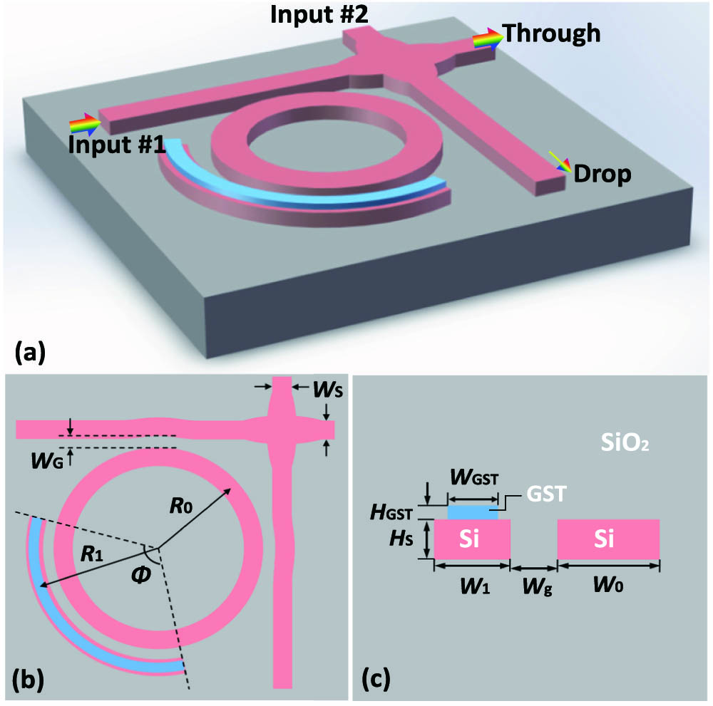
Figure 1.Schematic configuration of the proposed wavelength-selective photonic switch based on a GST-assisted MRR: (a) 3D view, (b) top view, (c) the cross section of the coupling region.
As an example, in this paper we choose the popular SOI waveguides with a 220 nm thick silicon core layer and a 2 μm thick buried silicon dioxide layer. The refractive indices of silicon and silica are and , respectively, at the central wavelength of 1550 nm. The complex refractive indices of GST are and [14], respectively, for the amorphous and crystalline states. For the microring waveguide, the radius is set as to guarantee a negligible bending loss and to achieve a large free spectral range (FSR).
As mentioned above, the microring waveguide and the bent GST-loaded silicon photonic waveguide are designed to satisfy the phase-matching condition [29,30] when the GST is in the crystalline state, which for concentric waveguides implies where and are the effective indices of the fundamental TE modes in the microring waveguide and the bent GST-loaded silicon photonic waveguide, respectively, and and are their bending radii. For these two concentric waveguides shown in Fig. 1(b), the bending radii are related with the gap width and the widths ( and ) of their silicon strips as follows:
For example, the width of the microring waveguide is set to according to the single-mode condition. The gap width is chosen as , which is sufficiently large to ensure high-quality filling of the upper cladding in the fabrication process. Since , one has according to the phase-matching condition, and thus one should make . Furthermore, regarding that GST has a higher refractive index than silicon, one should choose a thin GST layer. Otherwise, it is difficult to satisfy the phase-matching condition and one has to choose a very narrow GST strip. In our case, we choose the GST thickness as according to the fabrication process and the silicon-strip width . In order to determine the optimal GST-strip width according to the phase-matching condition, we calculate the product of the effective index and the bending radius of the bent GST-loaded silicon photonic waveguide as the GST width varies as shown in Fig. 2(a). Here the product for the microring waveguide is also given (see the red dashed line). From this figure, it can be seen that the optimal width for the GST strip is around , determined by the intersection of the two curves in Fig. 2(a).

Figure 2.(a) Calculated products of and for the fundamental TE mode as the GST-strip width varies. (b) Calculated transmission at the output end of the microring waveguide when the mode is launched from input end.
The bent directional coupler consisting of the microring waveguide and the GST-loaded silicon photonic waveguide is then optimized further by using a full-vectorial three-dimensional finite-difference time-domain (3D-FDTD) method. Figure 2(b) shows the calculated transmission at the output end of the microring waveguide when the mode is launched from input end. Here the angle of the bent coupling region is chosen as 90°, which is shorter than the coupling length and sufficiently long to determine the optimal GST-strip width for achieving maximal cross-coupling. As shown in Fig. 2(b), when the GST-strip width is chosen as 168 nm, the residual optical power in the microring waveguide is minimal, which indicates the optimal design for phase matching. On the other hand, it can be seen that the transmission is not sensitive to the GST-strip width, indicating that there is a large fabrication tolerance. As the cross-sectional parameters of the two optical waveguides in the coupling region are determined, the length of the coupling region is then optimized. First, the residual power in the microring waveguide should be minimized in the c-crystalline-GST (c-GST) state in order to strongly depress the resonance in the MRR and improve the extinction ratio of the switch. Meanwhile, the residual power in the microring waveguide should be maximized in the amphous-GST (a-GST) state to reduce the excess loss of the switch.
Figure 3(a) shows the transmissions at the output end of the microring waveguide when the fundamental TE mode launched from the input end goes through the coupling region as the coupling angle varies. Here the crystalline and amorphous states of GST are considered. It can be seen that the residual power in the microring waveguide decreases greatly as the coupling angle increases when it is with c-GST. This is expected in a coupling system with two phase-matched optical waveguides. For example, there is only 25% power left in the microring waveguide when , which is helpful to depress the resonance in the MRR. In contrast, for the amorphous state of GST, the cross-coupling is weak, and most power stays in the microring waveguide, which is also expected for a coupling system with two phase-mismatched optical waveguides. On the other hand, some oscillation is observed (see the solid blue line). This is because the phase mismatching is not very high while there is some coupling between the two waveguides placed closely. Nevertheless, one has a maximal residual power of 0.98 when . Correspondingly, the residual power in the microring waveguide for the c-GST state is about 0.35 (at ) as shown by the dashed line.
Figure 3.(a) Calculated transmission of the local coupling region for the two states of the GST as a function of the coupling angle. The inset shows the schematic configuration of the simulation model. Optical field distribution of the local coupling region simulated by the 3D-FDTD method in the GST (b) crystalline and (c) amorphous state. Here and .
Figures 3(b) and 3(c) show the FDTD-simulated light propagation in the designed coupling region consisting of the microring waveguide and the GST-loaded silicon photonic waveguide in the c-GST and a-GST states, respectively. Here the mode is launched from the straight waveguide connected with the microring waveguide and goes through the coupling region with an angle of . In order to reduce the reflection loss resulting from the abrupt junction at the input/output ends of the coupling region, waveguide tapers are introduced at both ends of the GST-loaded section. From Fig. 3(b), it can be seen that there is strong coupling from the microring waveguide to the GST-loaded silicon photonic waveguide as expected when it is in the c-GST state. In contrast, when it is in the a-GST state, light in the microring waveguide is coupled partially out to the GST-loaded silicon photonic waveguide and then coupled back as shown in Fig. 3(c). In this case, the total loss of the transmission is still low since the loss of the GST-loaded silicon photonic waveguide is low when it is with a-GST.
Figures 4(a) and 4(b) show the calculated spectral responses at the drop port and the through port of the designed MRR-based optical switch in the OFF (a-GST) and ON (c-GST) states when light is launched from input port #1. One has the same result when light is launched from input port #2. Here the spectral responses are calculated from a 3D-FDTD simulation. In this design, the width of the gap between the access optical waveguide and the microring waveguide is chosen as 220 nm, and the power coupling ratio is about 0.05. As shown in Fig. 4(a), when operating in the a-GST state, the MRR works with strong resonances, which is similar to those regular MRRs. In this case, the excess loss of the transmission at the drop port is about 2 dB for the resonance wavelength at around 1563 nm. This loss is mainly from the absorption loss of a-GST. When it is switched to the c-GST state, the resonance in the MRR is depressed greatly because of the high loss introduced by the coupling region with the GST-loaded silicon photonic waveguide as shown in Fig. 4(b). It can be seen that the peak power at the drop port is about . Meanwhile, the transmission at the through port has very shallow resonance dip, and the transmission loss is about 0.9 dB for the working wavelength, which exhibits strong resonance in the a-GST state. When comparing the results in Figs. 4(a) and 4(b), it can be seen that the resonance peaks/notches are depressed significantly when it is at the ON (c-GST) state, and the extinction ratio at the resonance wavelength is . In this case, it is not necessary to introduce large wavelength shift for achieving high extinction ratios, even though a slight wavelength shift of exists when the present device is switched from the a-GST state to the c-GST state. This is in principle different from those traditional MRR-based optical switches, which have a GST strip embedded in the cavity and a sufficiently large wavelength shift is indispensable. For example, the MRR-based optical switch demonstrated in Ref. [19] has a wavelength shift as large as 1.0 nm with a 13.5 dB switching contrast and 0.3 nm 3 dB bandwidth. Therefore, the present device allows relatively large 3 dB bandwidth ( in the present design) and relaxes the critical control of the operation wavelength (as required in those traditional ones), which is suitable for multichannel WDM systems. Figures 4(c) and 4(d) show the simulated light propagation in the designed optical switch when operating at the resonance wavelength near 1563 nm in the a-GST and c-GST states, respectively. As can be seen, when it is with a-GST (OFF), light is mainly dropped to the drop port, and very little power is residual at the through port. In contrast, when it operates with c-GST (ON), very little power is dropped, and light is mainly output from the through port. To verify the robustness of the designed switch, we have also analyzed the fabrication tolerances by assuming that the width of the GST strip has a dimensional deviation of . The simulation results show that the excess loss is increased by 0.7 dB and the extinction ratio degrades by 4.5 dB when , which is still acceptable. For the present wavelength-selective photonic switch, the working wavelength can be tuned to be aligned to the corresponding channel wavelength of WDM systems by using the techniques of laser trimming or thermal tuning when necessary, while the 3 dB bandwidth of the resonance peak can also be designed as desired by modifying the coupling ratio and the cavity loss. In order to further reduce the excess loss due to the GST absorption, one can replace GST with (GSST), which was developed recently as another new PCM with much lower absorption than GST [14]. This makes it possible to be extended for low-loss higher-port arrays.
Figure 4.Spectral responses of the designed microring switch simulated by the 3D-FDTD method in the GST (a) amorphous and (b) crystalline state. Optical power distribution of the designed microring switch at the resonance wavelength near 1563 nm in the GST (c) amorphous and (d) crystalline state.
3. CONCLUSION
In conclusion, we have proposed and designed a novel wavelength-selective optical switch based on a GST-assisted MRR, which consists of two access optical waveguides and a microring waveguide coupled with a bent GST-loaded silicon photonic waveguide. The present switch is switched ON by modifying GST from the amorphous state to the crystalline state. The microring waveguide and the bent GST-loaded silicon photonic waveguide are designed optimally according to the phase-matching condition so that high loss is introduced due to the strong coupling when it is in the c-GST state. As a result, the resonance in the MRR is depressed significantly. When it is off (a-GST), there is significant phase mismatching between the microring waveguide and the bent GST-loaded silicon photonic waveguide, and thus little coupling happens. In this case, the MRR works normally with strong resonances and one has a low-loss transmission at the drop port for the resonance wavelength. A 3D-FDTD simulation has been given for the optimal design of the photonic switches. The designed photonic switch has an extinction ratio of at the resonance wavelength, while the excess losses at the through port and drop port are 1–2 dB. Note that the resonance wavelength changes little when it is switched ON or OFF. This makes it suitable for multichannel dense wavelength-division-multiplexing (DWDM) systems. The nonvolatility of the PCM makes the present switch very attractive because of the low power consumption, which will be useful for switching and routing in photonic networks. The excess loss for the present wavelength-selective optical switch can be further reduced by replacing GST with GSST [14]. This makes it possible to be extended for low-loss higher-port arrays as well as other reconfigurable photonic integrated circuits.
References
[1] C. Sun, M. T. Wade, Y. Lee, J. S. Orcutt, L. Alloatti, M. S. Georgas, A. S. Waterman, J. M. Shainline, R. R. Avizienis, S. Lin, B. R. Moss, R. Kumar, F. Pavanello, A. H. Atabaki, H. M. Cook, A. J. Ou, J. C. Leu, Y. Chen, K. Asanović, R. J. Ram, M. A. Popović, V. M. Stojanović. Single-chip microprocessor that communicates directly using light. Nature, 528, 534-538(2015).
[2] Q. Cheng, M. Bahadori, M. Glick, S. Rumley, K. Bergman. Recent advances in optical technologies for data centers: a review. Optica, 5, 1354-1370(2018).
[3] Y. Arakawa, T. Nakamura. Silicon photonics for next generation system integration platform. IEEE Commun. Mag., 51, 72-77(2013).
[4] Q. Li, D. Nikolova, D. M. Calhoun, Y. Liu, R. Ding, T. Baehr-Jones, M. Hochberg, K. Bergman. Single microring-based 2 × 2 silicon photonic crossbar switches. IEEE Photon. Technol. Lett., 27, 1981-1984(2015).
[5] Q. Cheng, M. Bahadori, Y. Hung, Y. Huang, N. Abrams, K. Bergman. Scalable microring-based silicon Clos switch fabric with switch-and-select stages. IEEE J. Sel. Top. Quantum Electron., 25, 1-11(2019).
[6] A. S. P. Khope, M. Saeidi, R. Yu, X. Wu, A. M. Netherton, Y. Liu, Z. Zhang, Y. Xia, G. Fleeman, A. Spott, S. Pinna, C. Schow, R. Helkey, L. Theogarajan, R. C. Alferness, A. A. M. Saleh, J. E. Bowers. Multi-wavelength selective crossbar switch. Opt. Express, 27, 5203-5216(2019).
[7] S. Chen, Y. Shi, S. He, D. Dai. Low-loss and broadband 2 × 2 silicon thermo-optic Mach-Zehnder switch with bent directional couplers. Opt. Lett., 41, 836-839(2016).
[8] S. Wang, D. Dai. Polarization-insensitive 2 × 2 thermo-optic Mach-Zehnder switch on silicon. Opt. Lett., 43, 2531-2534(2018).
[9] Z. Guo, L. Lu, L. Zhou, L. Shen, J. Chen. 16 × 16 silicon optical switch based on dual-ring-assisted Mach-Zehnder interferometers. J. Lightwave Technol., 36, 225-232(2018).
[10] L. Qiao, W. Tang, T. Chu. 32 × 32 silicon electro-optic switch with built-in monitors and balanced-status units. Sci. Rep., 7, 42306(2017).
[11] W. Bogaerts, P. D. Heyn, T. V. Vaerenbergh, K. D. Vos, S. K. Selvaraja, T. Claes, P. Dumon, P. Bienstman, D. V. Thourhout, R. Baets. Silicon microring resonators. Laser Photon. Rev., 6, 47-73(2012).
[12] M. Wuttig, H. Bhaskaran, T. Taubner. Phase-change materials for non-volatile photonic applications. Nat. Photonics, 11, 465-476(2017).
[13] K. J. Miller, R. F. Haglund, S. M. Weiss. Optical phase change materials in integrated silicon photonic devices: review. Opt. Mater. Express, 8, 2415-2429(2018).
[14] Q. Zhang, Y. Zhang, J. Li, R. Soref, T. Gu, J. Hu. Broadband nonvolatile photonic switching based on optical phase change materials: beyond the classical figure-of-merit. Opt. Lett., 43, 94-97(2018).
[15] M. Rudé, J. Pello, R. E. Simpson, J. Osmond, G. Roelkens, J. J. G. M. van der Tol, V. Pruneri. Optical switching at 1.55 μm in silicon racetrack resonators using phase change materials. Appl. Phys. Lett., 103, 141119(2013).
[16] J. Zheng, A. Khanolkar, P. Xu, S. Colburn, S. Deshmukh, J. Myers, J. Frantz, E. Pop, J. Hendrickson, J. Doylend, N. Boechler, A. Majumdar. GST-on-silicon hybrid nanophotonic integrated circuits: a non-volatile quasi-continuously reprogrammable platform. Opt. Mater. Express, 8, 1551-1561(2018).
[17] M. Stegmaier, C. Ríos, H. Bhaskaran, C. D. Wright, W. H. P. Pernice. Nonvolatile all-optical 1 × 2 switch for chipscale photonic networks. Adv. Opt. Mater., 5, 1600346(2017).
[18] H. Zhang, L. Zhou, J. Xu, L. Lu, J. Chen, B. M. A. Rahman. All-optical non-volatile tuning of an AMZI-coupled ring resonator with GST phase-change material. Opt. Lett., 43, 5539-5542(2018).
[19] C. Wu, H. Yu, H. Li, X. Zhang, I. Takeuchi, M. Li. Low-loss integrated photonic switch using subwavelength patterned phase change material. ACS Photon., 6, 87-92(2018).
[20] N. Ali, R. Kumar. Design of a novel nanoscale high performance phase-change silicon photonic switch. Photon. Nanostr. Fundam. Appl., 32, 81-85(2018).
[21] H. Zhang, L. Zhou, L. Lu, J. Xu, N. Wang, H. Hu, B. M. A. Rahman, Z. Zhou, J. Chen. Miniature multilevel optical memristive switch using phase change material. ACS Photon., 6, 2205-2212(2019).
[22] N. Ali, R. Kumar. Mid-infrared silicon photonic switches using Ge2Sb2Te5 embedded in SOI waveguide. Nanotechnology, 31, 115207(2020).
[23] M. Jafari, M. Rais-Zadeh. Zero-static-power phase-change optical modulator. Opt. Lett., 41, 1177-1180(2016).
[24] Z. Yu, J. Zheng, P. Xu, W. Zhang, Y. Wu. Ultracompact electro-optical modulator-based Ge2Sb2Te5 on silicon. IEEE Photon. Technol. Lett., 30, 250-253(2018).
[25] C. Ríos, M. Stegmaier, P. Hosseini, D. Wang, T. Scherer, C. D. Wright, H. Bhaskaran, W. H. P. Pernice. Integrated all-photonic non-volatile multi-level memory. Nat. Photonics, 9, 725-732(2015).
[26] W. Zhang, R. Mazzarello, M. Wuttig, E. Ma. Designing crystallization in phase-change materials for universal memory and neuro- inspired computing. Nat. Rev. Mater., 4, 150-168(2019).
[27] M. Stegmaier, C. Ríos, H. Bhaskaran, W. H. P. Pernice. Thermo-optical effect in phase-change nanophotonics. ACS Photon., 3, 828-835(2016).
[28] Y. Ma, Y. Zhang, S. Yang, A. Novack, R. Ding, A. E. Lim, G. Lo, T. Baehr-Jones, M. Hochberg. Ultralow loss single layer submicron silicon waveguide crossing for SOI optical interconnect. Opt. Express, 21, 29374-29382(2013).
[29] M. K. Chin, S. T. Ho. Design and modeling of waveguide-coupled single-mode microring resonators. J. Lightwave Technol., 16, 1433-1446(1998).
[30] D. Dai, J. E. Bowers. Novel ultra-short and ultra-broadband polarization beam splitter based on a bent directional coupler. Opt. Express, 19, 18614-18620(2011).


