
Tianming Sun, Yu Xiao, Jinpeng Huo, Daozhi Shen, Wenxian Wang, Guisheng Zou. Nanojoining and Electrical Performance Modulation of Metal Oxide Nanowires Based on Femtosecond Laser Irradiation[J]. Chinese Journal of Lasers, 2021, 48(8): 0802006
- Chinese Journal of Lasers
- Vol. 48, Issue 8, 0802006 (2021)
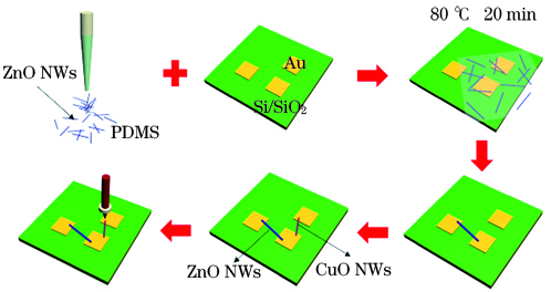
Fig. 1. Au electrode-nanowire heterostructure prepared by dry transfer method
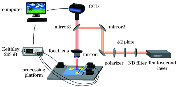
Fig. 2. Schematic diagram of the femtosecond laser processing system
Fig. 3. Surface morphology and phase structure of the nanowires. (a) SEM image of the CuO nanowires; (b) SEM image of the ZnO nanowires; (c) X-ray diffraction pattern of the CuO nanowires; (d) X-ray diffraction pattern of the ZnO nanowires
Fig. 4. Joint morphology of the heterostructure under different laser energy irradiation. (a) Au electrode-CuO nanowire heterostructure; (b) Au electrode-ZnO nanowire heterostructure
Fig. 5. Electric field intensity distribution under laser irradiation. (a) Au electrode-CuO nanowires; (b) Au electrode-ZnO nanowires; (c) electric field strength along the CuO nanowire axis and electrode contact surface; (d) electric field strength along the ZnO nanowire axis and electrode contact surface
Fig. 6. Electrical response before and after the nanowire is bonded to the Au electrode. (a),(c) Current output characteristics and transfer characteristics of the CuO nanowire FET devices before and after laser irradiation; (b),(d) current output characteristics and transfer characteristics of the ZnO nanowire FET devices before and after laser irradiation characteristic
Fig. 7. Semiconductor inverter based on p-CuO/n-ZnO nanowires. (a) Schematic structure of the inverter; (b) schematic circuit diagram; (c) OM image; (d) SEM image and EDS characterization of the p-CuO nanowire FET devices; (e) SEM image and EDS characterization of the n-ZnO nanowire FET devices
Fig. 8. Electrical response characteristics and energy band structure of the inverter. (a) Voltage and current transfer curve of the inverter in the initial state; (b)--(c) voltage and current transfer curves of the inverter after laser processing; (d) voltage regulation range of the inverter under different applied voltages; (e)--(f) energy band structure of p-CuO and n-ZnO nanowire FET under different gate voltages


Set citation alerts for the article
Please enter your email address

© Copyright 2018-2021 | Chinese Laser Press. All Rights Reserved 沪ICP备15018463号-20