• Chinese Optics Letters
  • Vol. 17, Issue 7, 072301 (2019)
Chenghao Lu, Bing Zhu, Chuanyi Zhu, Licheng Ge, Yian Liu, Yuping Chen*, and Xianfeng Chen
Author Affiliations
  • State Key Laboratory of Advanced Optical Communication Systems and Networks, School of Physics and Astronomy, Shanghai Jiao Tong University, Shanghai 200240, China
  • show less
    DOI: 10.3788/COL201917.072301 Cite this Article Set citation alerts
    Chenghao Lu, Bing Zhu, Chuanyi Zhu, Licheng Ge, Yian Liu, Yuping Chen, Xianfeng Chen. All-optical logic gates and a half-adder based on lithium niobate photonic crystal micro-cavities[J]. Chinese Optics Letters, 2019, 17(7): 072301 Copy Citation Text show less
    (a) Band diagrams in a square lattice PhC with LN (MgO-doped) rods for TE and TM modes. (b) The left is the schematic structure of the W1 waveguide in the Γ-M direction; the right is the FDTD simulation result of the W1 waveguide and the sketch of the light beam coherent interference.
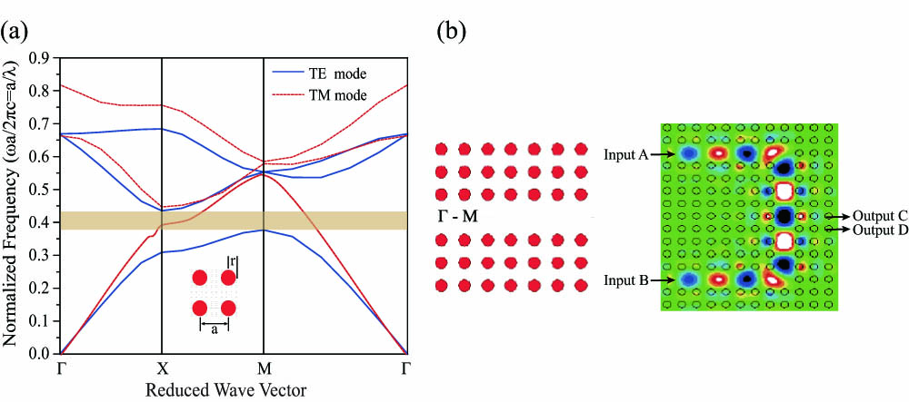
    Fig. 1. (a) Band diagrams in a square lattice PhC with LN (MgO-doped) rods for TE and TM modes. (b) The left is the schematic structure of the W1 waveguide in the Γ-M direction; the right is the FDTD simulation result of the W1 waveguide and the sketch of the light beam coherent interference.
    T-shape W1 waveguides (a) without or (b) with the L2 cavity in an LN PhC and the FDTD simulated different transmission results.
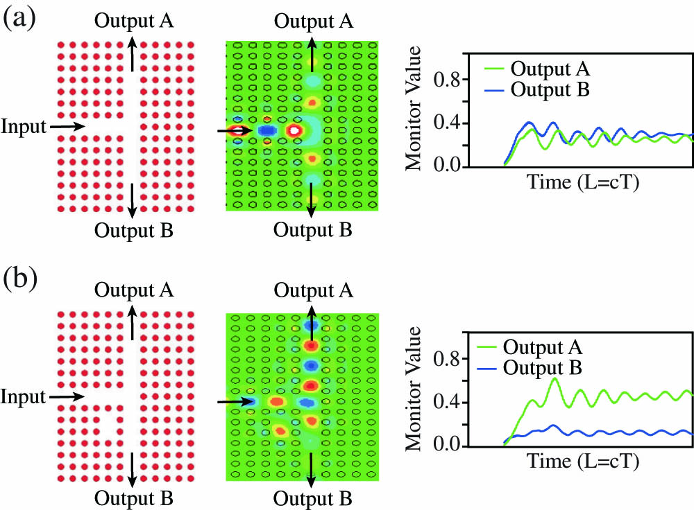
    Fig. 2. T-shape W1 waveguides (a) without or (b) with the L2 cavity in an LN PhC and the FDTD simulated different transmission results.
    Three all optical logic gates (a) AND, (b) XOR, and (c) NOT in an LN PhC with different micro-cavities locations.
    Fig. 3. Three all optical logic gates (a) AND, (b) XOR, and (c) NOT in an LN PhC with different micro-cavities locations.
    FDTD simulated transmission of (a) AND and (b) XOR gates in an LN PhC.
    Fig. 4. FDTD simulated transmission of (a) AND and (b) XOR gates in an LN PhC.
    (a) Schematic structure of the all-optical half-adder in an LN PhC. (b) The FDTD simulated transmission of the all-optical half-adder.
    Fig. 5. (a) Schematic structure of the all-optical half-adder in an LN PhC. (b) The FDTD simulated transmission of the all-optical half-adder.
    Input AInput BANDXORNOT
    0000\
    01011
    1001\
    11100
    Table 1. Truth Table for the AND, XOR, and NOT Logic Gates
    Input AInput BOutput C (Carry Digit)Output S (Sum Digit)
    0000
    0101
    1001
    1110
    Table 2. Truth Table for the All-optical Half-adder
    Chenghao Lu, Bing Zhu, Chuanyi Zhu, Licheng Ge, Yian Liu, Yuping Chen, Xianfeng Chen. All-optical logic gates and a half-adder based on lithium niobate photonic crystal micro-cavities[J]. Chinese Optics Letters, 2019, 17(7): 072301
    Download Citation