
Xiaozhe Ma, Fang Zhang, Huijie Huang. Correction Technology for Illumination Field Intensity Profile in Photolithography Machine[J]. Chinese Journal of Lasers, 2021, 48(20): 2005001
- Chinese Journal of Lasers
- Vol. 48, Issue 20, 2005001 (2021)
![Optical system structure of step-and-scan lithography[11-16]](/richHtml/zgjg/2021/48/20/2005001/img_1.jpg)
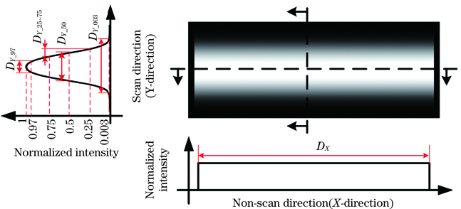
Fig. 2. Spatial distribution of top-Gaussian illumination field
Fig. 3. Generation principle of top-Gaussian illumination field
Fig. 4. In traditional illumination mode, the spot intensity distribution formed by a field point of view of the illumination light field on the light field correction plate. (a) Size of defocusing spot formation on the field correction plate; (b) intensity distribution of the defocusing spot on the field correction plate
Fig. 5. Simulation model of optical system for generating the top-Gaussian illumination field
Fig. 6. Illumination light field of three traditional lighting modes. (a) Illumination field 1; (b) illumination field 2; (c) illumination field 3
Fig. 7. Flow chart of transmittance distribution optimization algorithm of light field correction plate based on simulated annealing
Fig. 8. Tendency of Elost for three illumination fields during optimization. (a) Illumination field 1; (b) illumination field 2; (c) illumination field 3
Fig. 9. Transmittance distributions of three optimized correctors. (a) Corrector 1; (b) corrector 2; (c) corrector 3
Fig. 10. Comparison of the three illumination field intensity in non-scan and scan directions before and after correction. (a) Illumination field 1; (b) illumination field 2; (c) illumination field 3
Fig. 11. Simulation results of three corrected illumination fields. (a) Illumination field 1; (b) illumination field 2; (c) illumination field 3
| ||||||||||||||||||
Table 1. Requirements of the top-Gaussian illumination field
| ||||||||||||||||||||||||||||||||||||||||||||||||||
Table 2. Design results of the microlenses of MLAs and diffuser
| ||||||||||||||||||||||||||||||||||||||||||||||||||
Table 3. Pitch distributions of the microlenses of MLAs and diffuser
| ||||||||||||||||||||||||||||||||||
Table 4. Parameters of illumination light field of three traditional lighting modes
| ||||||||||||||||||||||||||||||||||||||||||
Table 5. Parameters and energy loss of the three corrected illumination fields (correction results in non-scan direction)
| ||||||||||||||||||||||||||||||||||||||||||
Table 6. Parameters and energy loss of the three corrected illumination fields (final corrected results)
| ||||||||||||||||||||||||||||||||||||||||||
Table 7. Parameters and energy loss of the three corrected lighting fields (simulation results)

Set citation alerts for the article
Please enter your email address
© Copyright 2018-2021 | Chinese Laser Press. All Rights Reserved 沪ICP备15018463号-20