In this work, we report a broadband terahertz wave modulator based on a top-gate graphene field effect transistor with polyimide as the gate dielectric on a PET substrate. The transmission of the terahertz wave is modulated by controlling the Fermi level of graphene via the polyimide as the top-gate dielectric material instead of the traditional dielectric materials. It is found that the terahertz modulator can achieve a modulation depth of with a small operating gate voltage of 3.5 V and a low insertion loss of 2.1 dB.
Graphene, a two-dimensional semi-metal with novel electronic properties, such as ultra-high carrier mobility and tunable density of its carrier states[1,2], has attracted extensive interest for applications in radio frequency devices, sensors, optoelectronic devices, and touch panels[3–5]. Technologies that generate, detect, and manipulate electromagnetic waves at the terahertz frequency have also been broadly investigated to fulfill their great potential in fundamental as well as in many practical applications, such as communications, radar, electronic countermeasures, imaging, and astronomy[6–14]. Recently, graphene has been used in terahertz technologies to make devices with superior performances over traditional materials, including terahertz plasma oscillators, waveguides, detectors, and modulators[15,16]. Among them, graphene field effect transistors (GFETs) can be used to tune the carrier concentration in graphene by applying a voltage at the gate, making it possible to modulate the absorption/transmission of terahertz waves through the devices[17–19]. In most GFET devices, was used as the gate dielectric on top of a -type silicon () substrate[17,20]. However, when used as a terahertz broadband modulator, GFET with a structure has drawbacks such as a low breakdown voltage, high operating voltage, and a high insertion loss.
Herein, we have demonstrated small operating voltage and low insertion loss terahertz modulators with the top-gate field effect transistor structure of graphene/polyimide (PI)/graphene/polyethylene terephthalate (PET), where terahertz modulation can be achieved through applying top-gate voltage. In contrast to terahertz modulators based on a GFET on an substrate, our device shows the following two outstanding characteristics: (1) the small operation gate voltage of can be obtained for the terahertz modulation depth of , which is attributed to the strong gate effect of PI with a higher capacitance, and (2) the low insertion loss of can be achieved, which is due to the small refractive index of the PET substrate.
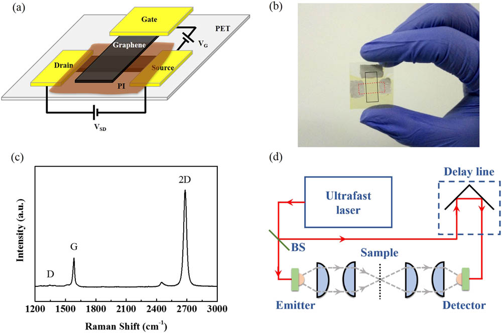
The schematic diagram and photograph of the terahertz modulator device based on a top-gate GFET are shown in Figs. 1(a) and 1(b), respectively. First, as the modulating layer, large-area monolayer graphene was synthesized by chemical vapor deposition on the copper foil and then was transferred onto the PET substrate (125 μm)[21,22]. Second, silver pastes were brushed as the source and drain electrodes, as shown in Fig. 1(a). The length and width of the device channel are and , respectively. Then, as the gate dielectric layer, PI liquid was spin coated onto the surface of the graphene channel of GFET at 3000 rpm. After that, PI liquid was baked at 80°C, 120°C, 150°C, and 180°C for 2 h to solidify it into PI film ()[23]. Finally, in order to avoid the influence of terahertz transmission from silver paste, another graphene strip was transferred onto the PI film as the top electrode and silver paste was brushed on the side of the graphene channel for the test. For this top-gate GFET structure, the carrier concentration of the under-layer graphene channel was modulated when different gate voltages were applied to the top-gate graphene electrode. Different from a terahertz modulator with PI as the dielectric layer and PET as substrate, a 285-nm substrate was employed to fabricate the terahertz modulator device based on a graphene back-gate FET. The of 285-nm thickness and were used as the dielectric layer and back gate electrode, respectively. The graphene channel with the same size as the top-gate modulator was transferred onto the substrate. Then the silver pastes were brushed on the two sides of the graphene channel as the source and drain electrodes.
Sign up for Chinese Optics Letters TOC. Get the latest issue of Chinese Optics Letters delivered right to you!Sign up now
Figure 1.(a) Schematic illustration of our top-gate GFETs. (b) The photograph of the terahertz modulator based on top-gate GFET. The boundaries of the channel of GFET and the top electrode with graphene are marked with red dotted lines and black solid lines, respectively. (c) Typical Raman spectrum of monolayer graphene transferred onto substrate. (d) Schematic of the experimental composition in our terahertz TDS system. The direction of the terahertz wave is incident from the graphene side and perpendicular to the surface of the terahertz modulator.
Raman spectroscopy was employed to investigate the quality of graphene used in our terahertz modulator[24,25]. The typical Raman spectrum of monolayer graphene transferred onto a 285-nm substrate is shown in Fig 1(c). The G to 2D peak intensity ratio () is , and the full-width at half-height maximum of the 2D peak is , suggesting monolayer graphene. The ratio of is below 0.1, indicating the high quality of the monolayer graphene used in the terahertz modulator. We measured the intensity modulation performance of the terahertz modulator by using a homemade fiber-coupled terahertz-time domain spectroscope (TDS), as shown in Fig. 1(d). The terahertz wave from the emitter is focused onto the center of the sample with a beam diameter of , covering the active area of the modulator[16]. In addition, in this work, it is noted that all transmittances of terahertz waves through the modulator have been normalized to the reference signal, which were measured without the modulator in air.
The modulation mechanism of the terahertz modulator based on the GFET can be explained as follows. In the terahertz range, the terahertz wave absorption by graphene is determined by the optical conductivity of graphene[26]. A higher optical conductivity corresponds to a lower terahertz transmission. In the terahertz modulator based on the GFET, the relationship between the optical conductivity and the DC electrical conductivity of graphene can be describe by Drude model as where is the DC electrical conductivity at the Fermi level , is the angular frequency of the photon, and is the carrier scattering time. In order to modulate the transmittance of the terahertz wave, a bias gate is applied to graphene through PI to vary the Fermi level of the graphene. When , the of graphene at the charge neutrality point (CNP), the carrier in graphene reaches the minimum, the of graphene reaches the minimum , and the absorption of the terahertz wave by graphene reaches the minimum , while the transmittance of the terahertz wave reaches the maximum . When (or ), the of graphene gradually moves away from the CNP to the conduction band (or to the valence band), the carrier in graphene increases, and the in graphene progressively increases, while the transmittance of the terahertz wave is reduced. The inset image of Fig. 2 shows the mechanism diagram of changing to modulate the Fermi level in graphene.
Figure 2.Total resistance as a function of the gate voltage in (a) PI- and (b) -based GFET.
Figure 2 shows the transfer characteristic curves of PI- and -based GFET, the total resistance () as a function of different back gate voltages . The maximum of PI-based GFET emerges at 3.5 V, where the CNP of this GFET device is, as shown in Fig. 2(a). At the CNP with 3.5 V gate voltage, the is at its maximum while the carrier concentration is minimized, which is consistent with the maximum transmittance of a terahertz wave. The electrical transport performance of -based GFET is also shown in Fig. 2(b). The CNP of -based GFET is , which is larger than that of PI-based GFET. This is because the graphene channel in the -based device was exposed to the air, which would cause the absorption of or , thus resulting the hole doping[22]. In contrast, for our PI-based terahertz graphene modulator, the PI coating on the graphene can effectively prevent the absorption of or , resulting in the CNP moving towards to 0 V and in the small value of (). The reason for the saturated resistance of the GFET on the PET substrate at a low gate bias voltage away from the CNP is mainly due to the reduction of mobility. The carrier concentration of graphene increases with the increasing gate bias voltage away from the CNP. The carrier scattering of graphene is enhanced by the increasing carrier concentration, resulting in the reduction of mobility. According to the following relations: , where is the mobility of graphene, is the carrier concentration, and is the resistivity of graphene, the resistance of the GFET tends to be saturated when the gate bias voltage moves away from the CNP[20]. Electrical measurements were carried out with an Agilent 4155B semiconductor parameter analyzer in air at room temperature.
To compare the terahertz modulation performance of PI- and -based GFET modulators, we measured the spectral transmission of these two modulators as shown in Fig. 3. Figure 3(a) shows the normalized intensity of the terahertz wave through the -based GFET structure from 0.1 to 1.1 THz under different gate voltages. A small modulation change in the terahertz wave transmission can be observed by electrical gating, where the back gate voltage varies from to 20 V. To study the maximum transmittance, here the modulation depth is defined as at 0.8 THz, where the transmittance has a minimum value of 27.1% at and a maximum value of 28.7% at 10 V. Consequently, the modulation depth of an -based terahertz graphene modulator can be calculated to be . Figure 3(b) shows the modulation curves measured for PI-based GFET. A distinctive variation in terahertz wave transmission was observed at different gate voltages from to 20 V. At 0.8 THz, the transmission exhibited a minimum of 61.5% at 0 V and reached a maximum of 77.8% at 3.5 V. The total modulation depth was calculated to be 20.9%.
Figure 3.Normalized intensity of transmitted terahertz wave through the (a) - and (b) PI-based GFET under different gate voltages. (c) The modulation depth of PI-based GFET as a function of the applied gate voltage. (d) The comparison of the amplitudes of the terahertz wave transmission through the - and PI-based GFETs at 0.8 THz.
Figure 3(c) shows the extracted modulation depth of PI-based GFET from 0.1 to 1.1 THz at different applied gate voltages. It is clear that the maximum modulation depth of 20.9% occurs at 0.8 THz at the top gate voltage of 0 V. It indicated that the transmission of the terahertz wave could be modulated precisely by applying the appropriate voltage. Figure 3(d) compares the amplitudes of terahertz waves at the frequency of 0.8 THz through the GFET with PI and gate dielectrics at different gate voltages. As shown in Fig. 3(d), the modulation of terahertz wave transmission can be greatly improved by employing PI as a dielectric material as opposed to in a terahertz graphene modulator.
Meanwhile, a much smaller operation voltage () is found in the terahertz graphene modulator with PI as he dielectric layer than in the terahertz graphene modulator with as the dielectric layer. Compared to the terahertz graphene modulator using as the gate dielectric, the modulator with PI as the gate dielectric has a more effective modulation efficiency. This would be attributed to the specific higher , which is described in[27]: where is the transconductance of the GFET, is the capacitance of the gate dielectric layer, is the voltage between the source and drain (1 V), and are the width and length of the graphene channel, and is the mobility of graphene. From Eq. (2), the change of is closely related to the value of by the relationship . The capacitance of PI is at 40 Hz, which is much larger than the typical values for 285 nm-thick () dielectrics. The larger capacitance of PI would provide a larger change of in GFET, and the more efficient modulation of the terahertz wave in this terahertz modulator under a smaller operating voltage. This is the reason for the more effective modulation efficiency in the terahertz modulator based on GFET with PI as the gate dielectric shown in Fig. 3[28,29]. It needs to be noted that, since the gate electrode is another layer of graphene, the carrier density in it also changes by the same amount but with a negative sign, as the two graphene layers and the PI film form a parallel plate capacitor. However, the change in the terahertz transmission is attributable to the change in the conductivity of the two graphene layers. As the top graphene layer is exposed in the atmosphere to and , which results in a -doped top graphene layer with a high carrier concentration at , the CNP of the top graphene layer is far away from , which is different from the CNP of the bottom graphene layer at a low gate voltage bias. In the range of low gate voltage biases, the conductivity of the exposed top graphene layer is almost unchanged, which is attributed to the increasing carrier concentration and the reductive carrier mobility. Therefore, the change of terahertz transmission is mainly influenced by the bottom graphene layer at a low gate voltage bias.
More important, a low insertion loss of terahertz wave was observed in our PI-based terahertz graphene modulator. Using air as the reference, Fig. 4(a) shows the transmittance of the PI-based terahertz modulator at 0 V gate voltage with the insertion loss of at 0.8 THz. The reason for the low insertion loss in the PI-based terahertz graphene modulator would be attributed to the PET substrate with a low insertion loss of at 0.8 THz, as shown in Fig. 4(a). However, the insertion loss of the -based terahertz graphene modulator is 5.6 dB, which is attributed to the high insertion loss of the () substrate in Fig. 4(b). The insertion loss of the PET substrate with a smaller refractive index () is much smaller than the substrate () with a higher refractive index (), as shown in Fig. 4(b). It is known that the attenuation is caused both by the reflection loss and absorption loss, and low-doped Si substrates have lower absorptions than PET. Thus, the smaller attenuation through the PET substrate can be attributed to the fact that PET has smaller reflection than low-doped Si substrates, which can be due to the lower value of the refractive index (1.65) of PET than that of Si (3.42). To realize devices with minimum insertion losses in a broad frequency range, employing a substrate with a lower refractive index is an effective method. Thus, the PI-based terahertz graphene modulator on the PET substrate would improve the effective utilization of the terahertz wave for practical applications.
Figure 4.(a) Transmittance and attenuation of PET and terahertz graphene modulator on PET substrate. (b) Transmittance and attenuation of and terahertz graphene modulator on the substrate.
In conclusion, we provide an effective method to fabricate a terahertz modulator based on a GFET using PI as the gate dielectric on a PET substrate with the modulation depth of under a small operating voltage () and a low insertion loss (). Compared to the -based terahertz modulator with the GFET structure, the PI-based terahertz modulator under a smaller operating voltage provides the more efficient modulation of the terahertz wave. This work is significant to provide a feasible method to decrease the operating voltage and improve the utilization of terahertz waves in terahertz technology applications.