• Photonics Research
  • Vol. 2, Issue 5, 102 (2014)
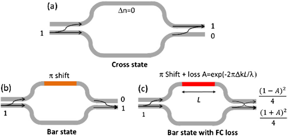
Richard Soref*
Author Affiliations
  • The Engineering Program, University of Massachusetts at Boston, 100 Morrissey Blvd., Boston, Massachusetts 02125, USA (Richard.Soref@umb.edu)
  • show less
    DOI: 10.1364/PRJ.2.000102 Cite this Article Set citation alerts
    Richard Soref, "Mid-infrared 2 × 2 electro-optical switching by silicon and germanium three-waveguide and four-waveguide directional couplers using free-carrier injection," Photonics Res. 2, 102 (2014) Copy Citation Text show less
    MZI 2×2 at (a) cross state with zero bias, (b) lossless bar state with π shift in one arm, and (c) bar state with π shift and free-carrier-induced loss in one arm.
    Fig. 1. MZI 2×2 at (a) cross state with zero bias, (b) lossless bar state with π shift in one arm, and (c) bar state with π shift and free-carrier-induced loss in one arm.
    MZI 2×2 bar-state IL (solid line) and CT (dashed line) versus ρ when ΔβL=π and Δk is induced in one arm.
    Fig. 2. MZI 2×2 bar-state IL (solid line) and CT (dashed line) versus ρ when ΔβL=π and Δk is induced in one arm.
    Top view of three-waveguide directional coupler 2×2 EO switch.
    Fig. 3. Top view of three-waveguide directional coupler 2×2 EO switch.
    4×4 crossbar matrix switch composed of 16 “2w” switches.
    Fig. 4. 4×4 crossbar matrix switch composed of 16 “2w” switches.
    4×4 permutation matrix switches made from six “3w” switches.
    Fig. 5. 4×4 permutation matrix switches made from six “3w” switches.
    4×4 permutation matrix switches made from six “4w” switches.
    Fig. 6. 4×4 permutation matrix switches made from six “4w” switches.
    Top view of 3w symmetric coupler with one central active waveguide and two adjoining passive waveguides. CW light is launched from WG1.
    Fig. 7. Top view of 3w symmetric coupler with one central active waveguide and two adjoining passive waveguides. CW light is launched from WG1.
    “2w” and “3w” 2×2 switching characteristics compared. The output of the two outer waveguides is shown as a function of phase shift induced in the central waveguide.
    Fig. 8. “2w” and “3w” 2×2 switching characteristics compared. The output of the two outer waveguides is shown as a function of phase shift induced in the central waveguide.
    Parameters of Si (a) 3w and (b) 4w used in 1.32 μm simulations.
    Fig. 9. Parameters of Si (a) 3w and (b) 4w used in 1.32 μm simulations.
    Beam-propagation simulation at 1.32 μm for Si 4w with (a) Lc=750 μm and (b) Lc=370 μm when Δn=Δk=0 (solid lines), ΔβL=14.3 and Δk=0 (dashed lines), and ΔβL=14.3 and ρ=Δn/Δk=10 (dotted lines).
    Fig. 10. Beam-propagation simulation at 1.32 μm for Si 4w with (a) Lc=750μm and (b) Lc=370μm when Δn=Δk=0 (solid lines), ΔβL=14.3 and Δk=0 (dashed lines), and ΔβL=14.3 and ρ=Δn/Δk=10 (dotted lines).
    (a) IL and (b) CT versus ΔβL in Si 3w (dashed line) and 4w (solid line) at 1.32 μm with coupling length engineered for Lc=750 μm. This is the lossless Δk=0 case.
    Fig. 11. (a) IL and (b) CT versus ΔβL in Si 3w (dashed line) and 4w (solid line) at 1.32 μm with coupling length engineered for Lc=750μm. This is the lossless Δk=0 case.
    Beam-propagation simulation at 1.32 μm for (a) Si 4w with Lc=750 μm and (b) 3w with Lc=1500 μm when Δn=Δk=0 (solid lines), Δn=0.004 and Δk=0 (dashed lines), and Δn=0.004 and Δk=0.001 (dotted lines).
    Fig. 12. Beam-propagation simulation at 1.32 μm for (a) Si 4w with Lc=750μm and (b) 3w with Lc=1500μm when Δn=Δk=0 (solid lines), Δn=0.004 and Δk=0 (dashed lines), and Δn=0.004 and Δk=0.001 (dotted lines).
    Bar-state IL and CT as a function of ρ for both switch configurations.
    Fig. 13. Bar-state IL and CT as a function of ρ for both switch configurations.
    Parameters of Ge (a) 3w and (b) 4w used in 12 μm simulations.
    Fig. 14. Parameters of Ge (a) 3w and (b) 4w used in 12 μm simulations.
    Beam-propagation simulation at 12 μm for (a) Ge 4w and (b) Ge 3w at zero bias (solid lines), lossless injection (dashed lines), and lossy injection (dotted lines).
    Fig. 15. Beam-propagation simulation at 12 μm for (a) Ge 4w and (b) Ge 3w at zero bias (solid lines), lossless injection (dashed lines), and lossy injection (dotted lines).
    λ (μm)Δne+ΔnhΔke+ΔkhΔβ(μm1)ρ=Δn/Δk
    1.320.00160.000090.007617.8
    1.550.00190.000120.007715.8
    20.00280.000190.008814.7
    50.01750.001400.022012.5
    70.03800.004400.03418.6
    120.11000.021000.05765.3
    Table 1. Change in Silicon Waveguide Core Index at a Carrier Injection Level of ΔNe=ΔNh=5×1017cm3
    λ (μm)Δne+ΔnhΔke+ΔkhΔβ(μm1)ρ=Δn/Δk
    20.00280.000870.00883.2
    50.01300.002700.01634.8
    70.03200.015000.02872.1
    120.06600.043000.03501.5
    Table 2. Change in Germanium Waveguide Core Index at a Carrier Injection Level of ΔNe=ΔNh=5×1017cm3
    λ (μm)Si 3w (μm)Si 4w (μm)Ge 3w (μm)Ge 4w (μm)
    1.3236841842
    1.5536361818
    23182153831821591
    512726361718859
    7822411976488
    12486243a800400a
    Table 3. Minimum Device Length in Si and Ge Required to Meet the ΔβL>28-for-3w and ΔβL>14-for-4w Criteria at the Carrier Injection Level of ΔNe=ΔNh=5×1017cm3
    Richard Soref, "Mid-infrared 2 × 2 electro-optical switching by silicon and germanium three-waveguide and four-waveguide directional couplers using free-carrier injection," Photonics Res. 2, 102 (2014)
    Download Citation