Key Laboratory of Artificial Micro- and Nano-structures of Ministry of Education of China, School of Physics and Technology, Wuhan University, Wuhan 430072, China
Fangqi Chen, Yong Liu, Tao Ding, "Fast and hydrosensitive switching of plasmonic nanocavities via photothermal effect," Photonics Res. 11, 12 (2023)
Copy Citation Text
Metallic nanoplasmonics, due to its extremely small size and ultrafast speed, has been one of the key components for next-generation information technology. It is vital that the highly tunable nanoplasmonic system in the solid state can be achieved for optoelectronic devices, which, still remains elusive for the visible region. Here we sandwich vanadyl oxalate () thin films in-between gold nanoparticles and gold film to establish thermo-responsive nanoantennas. The thickness of the composite films remains almost unchanged within the temperature cycles between 15°C and 80°C, while the refractive index of the films decreases with the increase of temperature due to the dehydration, which results in blueshift of the plasmon peak up to 60 nm. The plasmon resonances can be fully recovered when the temperature cools down again. This process is reversible within the temperature range of 15°C–80°C, which can be optically modulated with photothermal effect. Such thermo-responsive plasmonic nanoantenna works in the solid state with hundreds of kilohertz switching speed, which is highly compatible with traditional optoelectronic devices. It can be envisioned that this thermo-responsive optical thin film can be a promising candidate for integrated nanoplasmonic and optoelectronic devices.
1. INTRODUCTION
Optoplasmonic nanodevices are the key components to bridge the gap of integrated electronic circuits and optical chips for ultrafast optical information storage and processing [1]. One of the key aspects for their functionality is the facile and fast switchability of plasmon resonances to accommodate the demands of ultrasmall size and high operating speed [2], which, however, is nontrivial for conventional strategies.
One of the key obstacles is the compatibility issue of the current tunable plasmonic systems with the existing optoelectronic systems, which rules out most of the plasmon tuning systems based on wet (electro)chemistry [3–10]. An electric tunable plasmonic system appears more compatible but it adds up the complication of circuit designs and mostly operates in the infrared (IR) and terahertz regions [11,12]. An optically tunable plasmonic system is much superior in terms of simplicity, modulation speed, and ultrasmall sizes, making it a promising strategy towards the photonic chips. Although several optically addressable plasmonic systems have been proposed, the tunability of plasmons via this approach appears either irreversible [13–15] or in the infrared (IR)/terahertz regions [16–18]. For some systems, it has to be implemented in a liquid environment [19–22], which makes them far from practical applications.
Phase change materials such as germanium antimony telluride (GST) and vanadium dioxide () are commonly applied for nonvolatile memory devices [23,24]. However, due to their high phase transition temperature ( for GST, for ), it is a great challenge to integrate them into optoplasmonic nanosystems as such high local temperature may deform the plasmonic nanocomponents and surrounding dielectrics after cycles of operation [25,26], making their switchability vulnerable. Thus, most of their applications are limited to metasurfaces for propagating surface plasmons [27,28], whereas modulation of gap plasmons is rare [29,30].
Sign up for Photonics Research TOC. Get the latest issue of Photonics Research delivered right to you!Sign up now
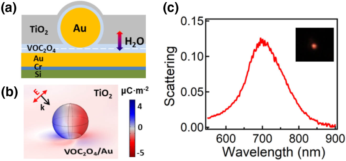
In this paper, we use vanadyl oxalate hydrates () films as the spacer in Au NP on mirror (NPoM) structure, which are capped by titanium dioxide () to maintain its stability in air [Fig. 1(a)]. The Au NPoM structure presents a dipolar mode of coupled plasmons due to its image charge [Fig. 1(b)] [31], which results in a coupled plasmon resonance in the scattering spectra [Fig. 1(c)]. Since this peak is very sensitive to the refractive index (RI) of the gap medium and the size of the nanocavity [32], we can modulate either of these two parameters to tune the plasmon resonances. As the films contain water molecules in a form of sol-gel matrix which can be dehydrated over time, the RI of such composite films can be modulated at ambient temperature. This RI tuning mechanism is totally different from the phase change material of which largely depends on the change of lattice symmetry at high temperature () [33,34]. Another unique advantage of using films is that their (de)hydration is reversible even at small thickness, which is critical to support the coupled gap plasmons of NPoM. The overlayer functionalizes as a water reservoir [35], which not only protects the layer from cracking but also supplies water molecules for the rehydration of the films when the temperature cools down, making plasmon shift fully reversible [Fig. 1(a)]. Such reversible shift of the plasmon resonances can also be optically controlled via photothermal effect, which unlocks a new type of thermo-responsive optical material that can be well integrated with optoplasmonic switches and optical chips of the next generation [36–38].
Figure 1.Design of thermo-responsive plasmonic system with films. (a) Scheme of Au NPoM with spacer and overcoated film. The white dashed line indicates another layer of coating. (b) Charge distribution profile of the Au NPoM with spacer (14 nm). (c) Scattering spectrum of an Au NPoM with 14 nm film in the gap. Inset is the dark field image of the Au NPoM.
The product of is obtained via the reduction of with [39]. The ethanol not only serves as solvent for the reaction system, but also facilitates the processing of ultrathin films via spin-coating (see Appendix A for experimental details). The reaction was monitored with UV-vis spectra, which suggests the reduction completes within 10 h [Figs. 2(a) and 2(b)]. The energy dispersive X-ray spectroscopy (EDS) of the films [Appendix B, Fig. 6(a)] indicates the presence of vanadium (V) with significant amounts of carbon (C) and oxygen (O), which were mainly originated from the oxalic acid. The valence state of V in the films is characterized by the X-ray photoemission spectroscopy (XPS), where the peaks of V and V exactly match the position of tetravalent vanadium [Fig. 2(c)] [40].
Figure 2.Synthesis of precursors and physicochemical analysis. (a) Production kinetics of monitored by UV-vis extinction spectra. (b) Change of the extinction intensity with reaction time. Inset is the picture of the sol-gel after 10 h reaction. (c) XPS profiles of films spin-coated on Si substrate. (d) XRD patterns of powders at 20°C and 80°C. (e) Change of the conductivity of films with one temperature cycle between 15°C and 80˚C. Inset is the electrode setup for the electric measurement. (f) Change of the conductivity of films within the temperature range of 40°C and 80°C.
The naturally dried powders are hydrated () as confirmed with the X-ray diffraction (XRD) patterns at room temperature [red line in Fig. 2(d)]. However, when the temperature rises to 80°C, the hydrates are reduced with only two water molecules per [blue line in Fig. 2(d)].
The loss of water molecules also changes its conductivity which shows temperature dependence [Figs. 2(e) and 2(f)]. The conductivity decreases dramatically when the temperature increases from 10°C to 30°C [Fig. 2(e)] but increases slightly as the temperature further increases over 40°C [Fig. 2(f)]. The first decrease of the conductivity is mainly due to the loss of surface absorbed water which significantly reduces the mobility of oxalic ions, while the slight increase at higher temperature is mainly due to the release of water molecules from the crystallites in the sol-gel films, which promotes the mobility of the oxalic ions again. When the temperature cools from 80°C to 10°C, its conductivity switches back with strong hysteresis as it takes time for reabsorption and diffusion of the water molecules.
Unlike other inorganic hydrates, the can be spin-coated on a flat substrate to form continuous thin films, which is due to the formation of O-V-O networks as evidenced by the weaker Raman mode of stretching compared to that of the crystallites in the powders [Appendix B, Fig. 6(b)]. Such a smooth thin film is temporarily sustained by the sol-gel matrix with free water molecules as the hydration layer to protect them from cracking. Longer time of aging in air can lead to dehydration and oxidation of the films, which can be avoided by spin-coating a protection layer of on top. Such composite films of have negligible strains at the interface as the sol-gel is highly reactive with , forming -Ti-O-V- networks at the interface between and via condensation [41]. This protective layer not only maintains the mechanical and chemical stability of the films but also stores the water molecules for films with humidity-responsive electric and optical properties.
For a proof-of-concept demonstration, we use as the spacer in the plasmonic nanostructures such as the Au NPoMs, which are protected by the films [Fig. 1(a)]. The atomic force microscope (AFM) images [Appendix B, inset of Fig. 6(c)] suggest the spacer is smooth and uniform with a thickness of as determined by ellipsometry [Appendix B, Fig. 6(c)]. A visible surface bump of only can be found with AFM imaging [Fig. 3(a)], suggesting successful overcoating of films on the Au NPoMs. The SEM image reveals the Au NPs are separated with a distance larger than 200 nm [Fig. 3(b)], excluding the possibility of interparticle coupling. This large separation also ensures the scattering spectra collected are from single Au NPoMs.
Figure 3.Temperature-responsive Au NPoM with composite films. (a) 3D AFM profile of the Au NPoM with medium overcoated with films. (b) SEM image of the Au NPoMs in film. (c) Change of scattering spectra of Au NPoM with temperature, and (d) the corresponding change of the plasmon resonances with one cycle of heating and cooling. (e) Reversible shift of plasmon resonances over several cycles of heating and cooling between 15°C and 50°C, and (f) the corresponding change of the resonance wavelength.
The plasmon resonance of the Au NPoM was monitored by dark field (DF) scattering spectra with a heating stage, which shows temperature-dependent property [Fig. 3(c)]. As the temperature increases from 15°C to 80°C, the plasmon resonance of the Au NPoM blueshifts from 730 to 670 nm, which can switch back to 730 nm after the temperature cools down to 15°C again [Fig. 3(d)]. This plasmon resonance is the dipolar mode of gap plasmons in Au NPoM as no obvious shift of the transverse mode () is observed if the Au mirror is replaced by the Si substrate (Appendix C, Fig. 7). Such a reversible switching process is very robust and can be cycled for over 10 times [Figs. 3(e) and 3(f)]. Moreover, the switching performance of this thermo-responsive plasmonic system can be maintained as long as proper sealing technique is applied, which can be nicely reproducible after 10 days (Appendix C, Fig. 8).
This reversible plasmon switching is mainly due to the change of RI as the thickness of films remains almost constant () throughout the thermal cycling from 15°C to 80°C [Appendix B, Fig. 6(d)]. The RI change of the films is mainly due to the loss of water molecules with rising temperature especially in the range from 10°C to 40°C (Fig. 4). Thermogravimetric analysis (TGA) of the powders shows the weight decreases linearly with increasing temperature but such a decrease clearly slows down in the temperature range from 45°C to 80°C [Fig. 4(a)]. The weight loss in the first phase (15°C to 45°C) is mainly due to the loss of absorbed free water molecules in powders, which correlates to the huge decrease of its conductivity [Fig. 2(e)]. After the temperature rises above 45°C, the almost all coverts to , which is very stable until the temperature reaches above 100°C [42]. By fitting of the curves in Fig. 4(a) we obtain the semi-empirical correlation between the weight of powders and the temperature () as
Figure 4.Comparison of the RI results measured from the TGA and SPR methods. (a) Change of weight ratio with temperature measured via TGA. (b) Change of surface relative humidity (RH) with temperature measured via a humidimeter. (c) Simulated change of SPR with RI. (d) Comparison of the RI measured from the TGA and SPR approaches.
Thus, the average RI change with temperature can be calculated with the formula where and are the RI of and , respectively. Thus, we can correlate the temperature with the RI of , which is presented as the dashed line in Fig. 4(d).
As for the films, the surface humidity can be roughly obtained with a humidimeter [Fig. 4(b)], which shows a similar trend to the powders [Fig. 4(a)], confirming the reliability of the TGA measurement. The correlation between the plasmon resonance and RI can be simulated with the finite element method (FEM) at a fixed gap size of [Fig. 4(c)]. By comparing the wavelength readings of the plasmon peak measured at different temperatures [Fig. 3(d)] to such correlation, we can obtain the relationship between the RI and temperature, which is shown as the red line in Fig. 4(d). We find that the RI obtained via surface plasmon resonance (SPR) method is close to the RI obtained by the TGA method. The slight deviation is mainly due to the differences on the packing and dimensions between powders and films. The excellent match of the results obtained from the TGA approach further manifests the reliability of SPR for RI sensing. This agreement also indicates the shift of plasmon is due to the change of RI induced by the change of water content in the gaps.
Normally, the shift of plasmon resonances induced by the RI change is small (); however, in this case, the shift of coupled plasmon resonances is large [up to 60 nm, Fig. 3(d)] since smaller nanogaps have higher sensitivity to the change of RI [Appendix C, Fig. 9(a)]. The current RI sensitivity of this hybrid NPoM system is 190 nm/RI unit with a figure of merit of 1.46.
Since the thermal effect can be locally delivered by plasmonic heating with a laser, such a reversible switching of coupled plasmons can be optically controlled with ultrafast response () [43,44]. To demonstrate the optical tunability of the coupled plasmons, another sample of Au NPoM was fabricated and irradiated with a 532 nm continuous wave (CW) laser, which can increase the local temperature of Au NPoM up to 30°C with a power of [Appendix C, Fig. 9(b)]. As a result, a blueshift of the coupled plasmons is observed from 676 to 664 nm [Fig. 5(a)] due to photothermally induced change of the local RI. Thus, reversible switching of plasmon resonances can be optically controlled at high modulation frequency of laser power, which persists robustly for many cycles [Fig. 5(b)], making it a promising prototype of optoplasmonic switching devices. The response time of such optical modulation is μ [Fig. 5(c)]. Power-dependent plasmon shift suggests that a critical threshold of is required for noticeable shift of plasmon resonances.
Figure 5.Laser-directed tuning of the plasmon resonances of Au NPoM coated with composite films. (a) Change of scattering spectra of Au NPoM with laser on and off (3 mW). (b) Change of the light scattering signal (integrated over 550–650 nm) in response to the square wave modulation of the CW laser. (c) Response-time of light-induced plasmon switching. (d) Scattering spectra of Au NPoM at different irradiation powers. (e) Change of the resonance wavelength with laser power.
Both the response time and tuning range are critical parameters of optoplasmonic devices. In addition, the compatibility with existing optoelectronic systems is also an important factor to consider. Here we make a brief comparison of the -based optoplasmonic system to other optically tunable plasmonic systems based on different types of materials (Table 1). Responsive polymers such as poly(N-isopropylacrylamide) (PNIPAM) are commonly applied for plasmon tuning which shows large tuning range and excellent reversibility [15,21]; however, it has to be implemented in an aqueous environment which deters their application in optoplasmonic chips. Other electric- and light-responsive polymers such as azobenzene-doped poly(methyl methacrylate) (AZO/PMMA) [45] and polyvinyldifloride (PVDF) [46] although can be tuned in the solid state, their reversibility is mediocre. Liquid crystals (LCs) [47] are a class of commercialized optical materials which have been widely applied to modulate the plasmon resonances but their tuning range is always small with relatively slow response time (). Phase change materials such as GST [29,48] and [49,50] may be more integratable to the optoelectronic devices with features of high speed and large tuning range, but they mainly work in a spectrum over IR. Thus, this material system we demonstrated here complements the traditional phase change materials in terms of working range without losing the typical features of large tunability and fast switching speed, making it a promising prototype of optoplasmonic sensing and nanophotonic devices.
Comparison of This Work to Other Typical Tunable Nanoplasmonic Systems
Materialsa
Tuning Range (nm)
Reversibility
Response Time (s)
Chip Compatibility
References
PNIPAM
655–710615–640
Good
Poor
[15,21]
AZO/PMMA
634–664
Poor
Good
[45]
PVDF
710–763
Poor
–
Good
[46]
LCs
1008–1027
Good
Good
[47]
GST
1060–10854770–5350
Good
Good
[29,48]
1100–12001068–1878
Good
Good
[49,50]
680–740
Good
Good
This work
The materials indicated here are the surrounding media of different plasmonic nanostructures.
3. CONCLUSIONS
In summary, we have established a temperature-responsive plasmonic system based on inorganic thin films of . These inorganic thin films function as a spacer in the Au NPoMs, whose RI decreases as the temperature increases, resulting in a blueshift of plasmon resonance as supported by simulations. The films can be rehydrated when the temperature drops, which redshifts the plasmon peak back again. This process is reversible for many thermal cycles, which can also be photothermally switched with laser illumination. Such temperature-responsive plasmons with solid-state thin films have great compatibility with optoelectronic devices, which can potentially be applied in optoplasmonic switches with ultrafast response.
Acknowledgment
Acknowledgment. We thank the support of the Center for Nanoscience and Nanotechnology at Wuhan University. We also thank Dr. Huatian Hu for his assistance on the simulation.
APPENDIX A: EXPERIMENTAL METHODS
Preparation of <inline-formula><math display="inline" id="m98" xmlns:mml="http://www.w3.org/1998/Math/MathML"><mrow><msub><mrow><mi>VOC</mi></mrow><mn>2</mn></msub><msub><mi mathvariant="normal">O</mi><mn>4</mn></msub></mrow></math></inline-formula> and <inline-formula><math display="inline" id="m99" xmlns:mml="http://www.w3.org/1998/Math/MathML"><mrow><msub><mrow><mi>TiO</mi></mrow><mn>2</mn></msub></mrow></math></inline-formula> Sol-gel Solutions
The sol-gel solution was prepared by mixing oxalic acid dihydrate ( obtained from Bidepharm) and vanadium pentoxide ( purchased from Macklin) in a molar ratio of 3:1 with 10 mL ethanol solution. This sol-gel mixture was further refluxed at 120°C for 10 h until a transparent blue solution of was obtained [39]. This reaction process was monitored with a UV-vis optofiber spectrometer (QE65000, Ocean Optics). This blue solution was further filtered to remove any insoluble impurities, which was then diluted by 15 times for stock use (shelf life: 2 days). The sol-gel solution was prepared by adding 2.5 mL of titanium butoxide, 156 μL of (1 mol/L), and 78 μL of to 25 mL isopropanol solution under magnetic stirring in a 50 mL flask overnight at room temperature.
Fabrication of Au NPoM with <inline-formula><math display="inline" id="m107" xmlns:mml="http://www.w3.org/1998/Math/MathML"><mrow><msub><mrow><mi>VOC</mi></mrow><mn>2</mn></msub><msub><mi mathvariant="normal">O</mi><mn>4</mn></msub></mrow></math></inline-formula> Spacer
The Au films were fabricated by thermal evaporation on Si substrate with thickness of 70 nm at the rate of Å. An ultrathin layer of film is spin-coated on the Au films at the speed of 4000 r/min for 40 s, followed by drop-casting 80 nm Au NPs (from BBI solutions) on top. Another layer of was successively spin-coated on top of the Au NPs to fully encapsulate the Au NPs in the films. At last, a layer of was spin-coated on top of the films for protection.
Tuning Coupled Plasmons with Thermo-Responsive <inline-formula><math display="inline" id="m114" xmlns:mml="http://www.w3.org/1998/Math/MathML"><mrow><msub><mrow><mi>VOC</mi></mrow><mn>2</mn></msub><msub><mi mathvariant="normal">O</mi><mn>4</mn></msub></mrow></math></inline-formula> Films
The Au NPoM samples were placed on a Peltier stage (Linkam P90) with temperature control (10°C–80°C) under a DF optical microscope. The relative humidity was maintained above 40% for the proper functionality of the device. The scattering spectra of each individual Au NPoM were collected at different temperatures through a DF objective (Olympus, ), which was coupled confocally with a optofiber spectrometer (integration time: 800 ms, QEPro, Ocean Optics). As for the light-induced photothermal tuning of the coupled plasmons, a 532 nm CW laser was focused on the Au NPoM, and the DF scattering and photoluminescence signals were collected by the spectrometer with a 550 nm long-pass filter (LP550, Thorlabs).
Characterizations
The crystalline property of the powders was characterized by XRD with a scanning rate of 7(°)/min from 15° to 50° (D8 Brucker, Karlsruhe, Germany). TGA measurements were performed (empty crucible as reference sample) at the scanning rate of 10°C/min (DSC3/TGA2, Mettler-Toledo). SEM (Sigma Zeiss) images and EDS of films were captured at the acceleration voltages of 5 kV and 20 kV, respectively. The valence states of the elements in the samples were determined by XPS (ESCALAB 250Xi, Thermo Fisher Scientific, Waltham, MA, USA). The RI and thickness of the films were determined with ellipsometry (, J. A. Woollam). All AFM measurements were done with a commercial Nanosurf LensAFM. The topographical measurements were done in tapping mode with a scan speed of 1 line/s. Electric conductance of the hybrid films was measured with cross-finger electrodes [inset of Fig. 2(e)] at a basic voltage of 1 V (Keithley 2635B).
Simulations
The temperature distributions around the Au NPs were simulated based on solving the Laplace equation using FEM. The RI of is set as 1.8. Johnson-Christy and Aspnes are adopted for the RI of Au and Si, respectively. The thermal conductivities of Au and are 318 and , respectively. The scattering spectra of the Au NPoMs were calculated via FEM at vaired RIs around the Au NP from 1.4 to 2.0, whose peak wavelengths were extracted to establish the correlation between plasmon resonance and RI [Fig. 4(c)].
APPENDIX B: CHARACTERIZATIONS OF VOC2O4 FILMS
The EDS of the films [Fig. 6(a)] shows the presence of V, C, and O elements, and Raman spectra in Fig. 6(b) show that films present a much weaker Raman mode of V = O stretching than the powders.
Ellipsometry spectra [Fig. 6(c)] indicate the thickness of films is about 14 nm, showing smooth and uniform surfaces as revealed by AFM [Insets of Fig. 6(c)]. The whole films keep almost constant thickness of 14 nm throughout the temperature cycles [Fig. 6(d)].
Figure 6.Characterizations of films. (a) EDS spectrum of films on Si substrate. (b) Raman spectra of powder and films. (c) Ellipsometry spectra of films spin-coated on Au substrate. Insets are AFM images of Au films with and without overcoating. (d) Change of film thickness with temperature.
APPENDIX C: TEMPERATURE-RESPONSIVE PLASMONS OF Au NPS WITH VOC2O4 FILMS AND SIMULATIONS
The scattering spectra of Au NPs coated with composite films on Si substrate show no obvious shift of plasmons with the change of temperature (Fig. 7) as this plasmon mode is localized plasmon resonance which is less sensitive to the change of RI as compared to the coupled plasmon mode. For the coupled plasmons, it can maintain robust switching performance even after 10 days (Fig. 8).
Figure 7.Change of scattering spectra of Au NPs coated with composite films on Si substrate.
Figure 8.Thermal switching performance of Au NPoM with composite films measured after 10 days. (a) Reversible shift of plasmon resonances over several cycles of heating and cooling between 15°C and 50°C, and (b) the corresponding change of resonance wavelength.
Figure 9.Theoretical simulations of the change of (a) the SPR wavelength with RI at different gaps and (b) the surface temperature of Au NPoM with irradiation power. Laser wavelength: 532 nm.
[42] J. Zhang, Z. W. Zhu, Z. Lei, L. N. Wang, D. S. Chen, A. F. Yi, H. Su, T. Qi. Preparation of vanadium oxalate by solvent extraction and purification with P507 and its physicochemical properties. Chem. J. Chin. Univ., 4, 740(2019).