• Acta Physica Sinica
  • Vol. 68, Issue 23, 237303-1 (2019)
Guo-Xiang Chen1、*, Xiao-Bo Fan1, Si-Qi Li1, and Jian-Min Zhang2
Author Affiliations
  • 1School of Science, Xi’an Shiyou University, Xi’an 710065, China
  • 2School of Physics and Information Technology, Shanxi Normal University, Xi’an 710062, China
  • show less
    DOI: 10.7498/aps.68.20191246 Cite this Article
    Guo-Xiang Chen, Xiao-Bo Fan, Si-Qi Li, Jian-Min Zhang. First-principles study of magnetic properties of alkali metals and alkaline earth metals doped two-dimensional GaN materials[J]. Acta Physica Sinica, 2019, 68(23): 237303-1 Copy Citation Text show less
    Geometry of alkali and alkali-earth metals doped GaN monolayer: (a) Top view; (b) side view.碱金属和碱土金属掺杂GaN单层结构图 (a) 俯视图; (b) 侧视图
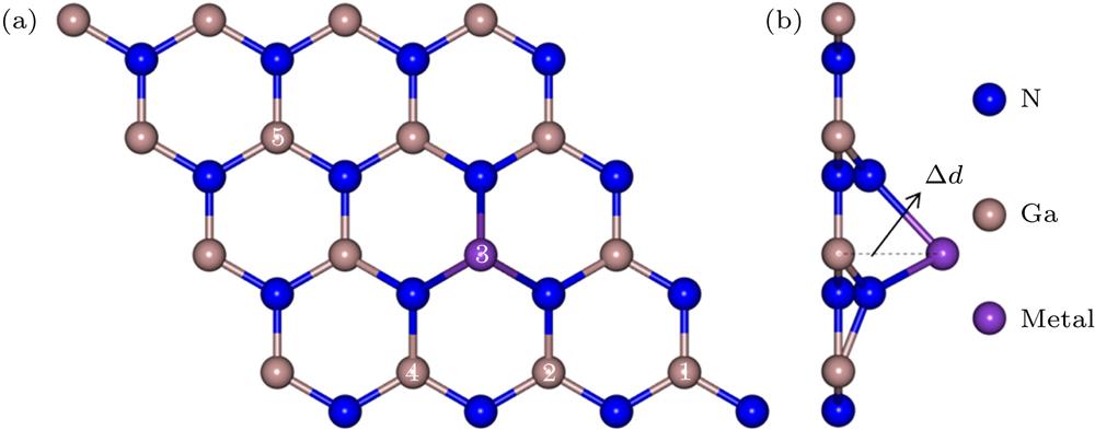
    Fig. 1. Geometry of alkali and alkali-earth metals doped GaN monolayer: (a) Top view; (b) side view.碱金属和碱土金属掺杂GaN单层结构图 (a) 俯视图; (b) 侧视图
    Spin charge density distributions of single atom doped GaN monolayer, isosurface is 0.004 eV/Å: (a) Li doping; (b) Na doping; (c) K doping; (d) Rb doping; (e) Be doping; (f) Mg doping; (g) Sr doping.单原子掺杂GaN单层的自旋电荷密度分布图, 等值面为0.004 eV/Å (a) Li掺杂; (b) Na掺杂; (c) K掺杂; (d) Rb掺杂; (e) Be掺杂; (f) Mg掺杂; (g) Sr掺杂
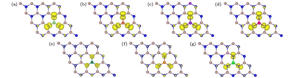
    Fig. 2. Spin charge density distributions of single atom doped GaN monolayer, isosurface is 0.004 eV/Å: (a) Li doping; (b) Na doping; (c) K doping; (d) Rb doping; (e) Be doping; (f) Mg doping; (g) Sr doping.单原子掺杂GaN单层的自旋电荷密度分布图, 等值面为0.004 eV/Å (a) Li掺杂; (b) Na掺杂; (c) K掺杂; (d) Rb掺杂; (e) Be掺杂; (f) Mg掺杂; (g) Sr掺杂
    Spin resolved total DOS and PDOS of GaN monolayer doped single-atom: (a) Pristine; (b) Li doping; (c) Na doping; (d) K doping; (e) Rb doping; (f) Be doping; (g) Mg doping; (h) Sr doping.单原子掺杂GaN单层的自旋DOS和PDOS图 (a) 未掺杂; (b) Li掺杂; (c) Na掺杂; (d) K掺杂; (e) Rb掺杂; (f) Be掺杂; (g) Mg掺杂; (h) Sr掺杂
    Fig. 3. Spin resolved total DOS and PDOS of GaN monolayer doped single-atom: (a) Pristine; (b) Li doping; (c) Na doping; (d) K doping; (e) Rb doping; (f) Be doping; (g) Mg doping; (h) Sr doping.单原子掺杂GaN单层的自旋DOS和PDOS图 (a) 未掺杂; (b) Li掺杂; (c) Na掺杂; (d) K掺杂; (e) Rb掺杂; (f) Be掺杂; (g) Mg掺杂; (h) Sr掺杂
    Band structures for single atom doped GaN monolayer, the blue and the red respectively represent the spin up and the spin down: (a) Pristine; (b) Li doping; (c) Na doping; (d) K doping; (e) Rb doping; (f) Be doping; (g) Mg doping; (h) Sr doping.单原子掺杂GaN单层的能带结构, 图中蓝与红分别代表自旋向上与向下 (a) 未掺杂; (b) Li掺杂; (c) Na掺杂; (d) K掺杂; (e) Rb掺杂; (f) Be掺杂; (g) Mg掺杂; (h) Sr掺杂
    Fig. 4. Band structures for single atom doped GaN monolayer, the blue and the red respectively represent the spin up and the spin down: (a) Pristine; (b) Li doping; (c) Na doping; (d) K doping; (e) Rb doping; (f) Be doping; (g) Mg doping; (h) Sr doping.单原子掺杂GaN单层的能带结构, 图中蓝与红分别代表自旋向上与向下 (a) 未掺杂; (b) Li掺杂; (c) Na掺杂; (d) K掺杂; (e) Rb掺杂; (f) Be掺杂; (g) Mg掺杂; (h) Sr掺杂
    (a) Top and side views of a local structure centered on the nearest neighboring N atom of the doped atom; (b) schematic diagram of the energy-level splitting and electron filling of the nearest N atom of the Li, Be-doped atom.(a) 掺杂原子最近邻N原子为中心的局部结构俯视图和侧视图; (b) Li, Be掺杂原子最近邻N原子能级劈裂及电子填充示意图
    Fig. 5. (a) Top and side views of a local structure centered on the nearest neighboring N atom of the doped atom; (b) schematic diagram of the energy-level splitting and electron filling of the nearest N atom of the Li, Be-doped atom.(a) 掺杂原子最近邻N原子为中心的局部结构俯视图和侧视图; (b) Li, Be掺杂原子最近邻N原子能级劈裂及电子填充示意图
    The p-orbital DOSs of the nearest neighbor N atom of doped atom: (a) Pristine; (b) Li doping; (c) Na doping; (d) K doping; (e) Rb doping; (f) Be doping; (g) Mg doping; (h) Sr doping.掺杂原子最近邻N原子的p轨道态密度图 (a) 未掺杂; (b) Li掺杂; (c) Na掺杂; (d) K掺杂; (e) Rb掺杂; (f) Be掺杂; (g) Mg掺杂; (h) Sr掺杂
    Fig. 6. The p-orbital DOSs of the nearest neighbor N atom of doped atom: (a) Pristine; (b) Li doping; (c) Na doping; (d) K doping; (e) Rb doping; (f) Be doping; (g) Mg doping; (h) Sr doping.掺杂原子最近邻N原子的p轨道态密度图 (a) 未掺杂; (b) Li掺杂; (c) Na掺杂; (d) K掺杂; (e) Rb掺杂; (f) Be掺杂; (g) Mg掺杂; (h) Sr掺杂
    (a) Spin charge density distribution of the Mg-doped C4 configuration, the isosurface is 0.02 eV/Å; (b) PDOS of Mg-2p, 1N-2p, 2N-2p and 3N-2p in the Mg-doped C4 configuration.(a) Mg掺杂C4构型的自旋电荷密度分布图, 等值面为0.02 eV/Å; (b) Mg掺杂C4构型中Mg-2p, 1N-2p, 2N-2p和3N-2p的PDOS
    Fig. 7. (a) Spin charge density distribution of the Mg-doped C4 configuration, the isosurface is 0.02 eV/Å; (b) PDOS of Mg-2p, 1N-2p, 2N-2p and 3N-2p in the Mg-doped C4 configuration.(a) Mg掺杂C4构型的自旋电荷密度分布图, 等值面为0.02 eV/Å; (b) Mg掺杂C4构型中Mg-2p, 1N-2p, 2N-2p和3N-2p的PDOS
    Metals$\Delta E$/eV $\Delta d$dM—N${E_{{\rm{form}}}}$/eV ${M_{\rm{N}}}/{\mu _{\rm{B}}}$${M_{{\rm{tot}}}}/{\mu _{\rm{B}}}$
    Ga-richN-rich
    Li0.2951.1271.9723.5223.3030.5432
    Na1.2021.8742.3054.2244.0050.5212
    K2.4362.4822.6573.7343.5150.5312
    Rb3.0762.6752.7963.3703.1510.5252
    Be0.0000.0001.6790.5820.3630.2181
    Mg0.0890.7661.9573.8213.6020.1981
    Sr1.9562.0312.3821.3241.1050.2391
    Table 1. Energy difference , distance from the doped atom to the GaN monolayer , optimized M—N bond length dM—N, formation energy of doped system , magnetic moment of the nearest three N atoms around the doped atom and total magnetic moment of doped system . 两种掺杂模式的能量差 , M原子到GaN单层的距离 , 优化后M—N键长dM—N, 体系形成能 , 三个最近邻N原子磁矩 和体系总磁矩
    MetalsConfigurations${d_{{\rm{M}} - {\rm{M}}}}$${E_{{\rm{RS}}}}$/eV $\Delta E$/eV ${M_{ {\rm{tot} } } }/{\mu _{\rm B}}$Coupling
    LiC1 (1, 2)3.3150.0000.3134FM
    C2 (1, 3)5.6630.3180.0494FM
    C3 (1, 4)6.4750.2220.5964FM
    C4 (1, 5)11.2150.2220.0344FM
    NaC1 (1, 2)3.6620.0000.3084FM
    C2 (1, 3)5.7060.3290.0334FM
    C3 (1, 4)6.4750.2160.4814FM
    C4 (1, 5)11.2150.2160.0144FM
    KC1 (1, 2)4.1470.0000.3184FM
    C2 (1, 3)5.7890.2760.0324FM
    C3 (1, 4)6.4750.1420.2394FM
    C4 (1, 5)11.2150.1420.0224FM
    RbC1 (1, 2)4.3260.0000.3224FM
    C2 (1, 3)5.8420.2720.0964FM
    C3 (1, 4)6.4750.1370.2404FM
    C4 (1, 5)11.2150.1370.0194FM
    BeC1 (1, 2)3.1680.0680.2892FM
    C2 (1, 3)5.5970.0000.0002FM
    C3 (1, 4)6.4750.1000.1482FM
    C4 (1, 5)11.2150.1000.1192FM
    MgC1 (1, 2)3.3590.0000.2412FM
    C2 (1, 3)5.6510.035–0.0032FM
    C3 (1, 4)6.4750.0800.0682FM
    C4 (1, 5)11.2150.0790.1682FM
    SrC1 (1, 2)4.0920.0490.1942FM
    C2 (1, 3)5.8680.1240.0762FM
    C3 (1, 4)6.4750.000–0.0020AFM
    C4 (1, 5)11.2150.0020.3522FM
    Table 2. Distance between the two doped atoms after structural optimization , relative stability of the four configurations , energy difference between AFM and FM , total magnetic moment of doped system , coupling is the magnetic coupling of various configurations of double M atom doped GaN monolayer. 结构优化后两掺杂原子的距离 , 4种构型相对稳定能 , AFM与FM的能量差 , 掺杂体系总磁矩 , coupling为双M原子掺杂的GaN纳米片各构型的磁耦合态
    Guo-Xiang Chen, Xiao-Bo Fan, Si-Qi Li, Jian-Min Zhang. First-principles study of magnetic properties of alkali metals and alkaline earth metals doped two-dimensional GaN materials[J]. Acta Physica Sinica, 2019, 68(23): 237303-1
    Download Citation