
Lingling Xie, Bingkun Chen, Fa Zhang, Ziheng Zhao, Xinxin Wang, Lijie Shi, Yue Liu, Lingling Huang, Ruibin Liu, Bingsuo Zou, Yongtian Wang. Highly luminescent and stable lead-free cesium copper halide perovskite powders for UV-pumped phosphor-converted light-emitting diodes[J]. Photonics Research, 2020, 8(6): 768
- Photonics Research
- Vol. 8, Issue 6, 768 (2020)
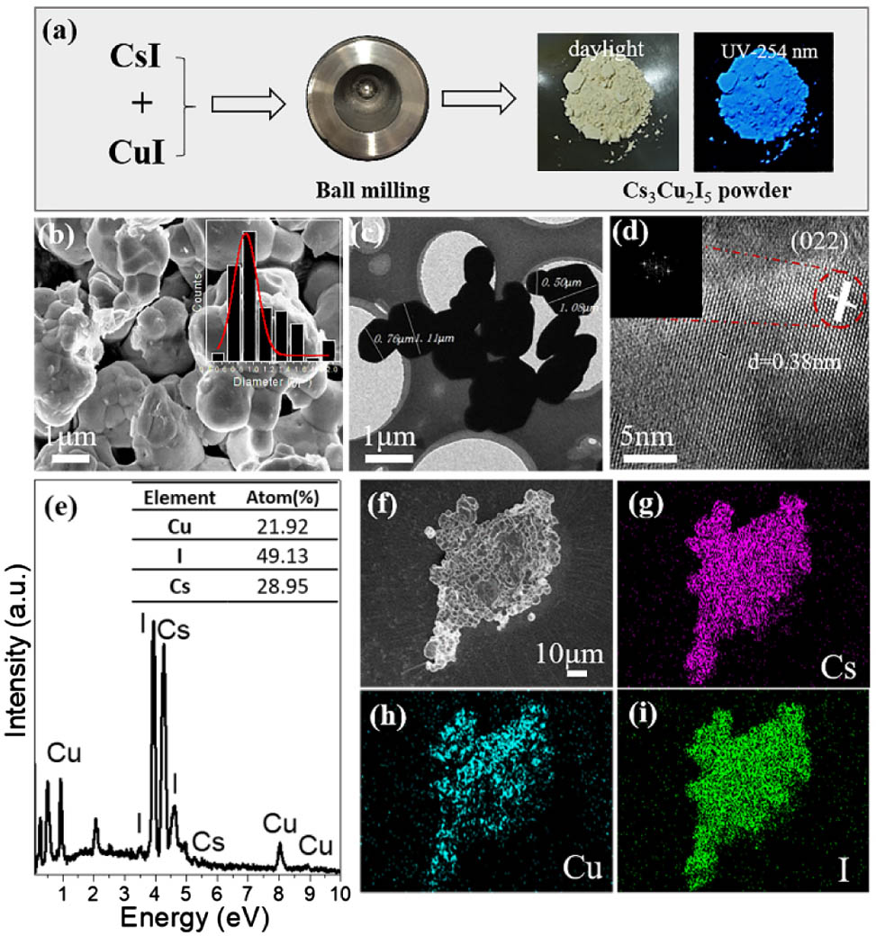
Fig. 1. (a) Schematic illustration of synthetic process of Cs 3 Cu 2 I 5 Cs 3 Cu 2 I 5 Cs 3 Cu 2 I 5 Cs 3 Cu 2 I 5 Cs 3 Cu 2 I 5 Cs 3 Cu 2 I 5 Cs 3 Cu 2 I 5
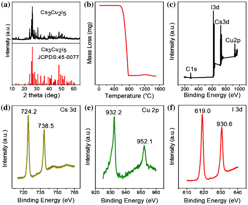
Fig. 2. (a) XRD pattern of obtained Cs 3 Cu 2 I 5 Cs 3 Cu 2 I 5 Cs 3 Cu 2 I 5 Cs 3 Cu 2 I 5
Fig. 3. (a) PL spectra of Cs 3 Cu 2 I 5 Cs 3 Cu 2 I 5 Cs 3 Cu 2 I 5 Cs 3 Cu 2 I 5 a Cs 3 Cu 2 I 5 Cs 3 Cu 2 I 5 E = 0
Fig. 4. (a) Integrated PL intensity as a function of temperatures from 25°C to 300°C. Variation of PL intensity of Cs 3 Cu 2 I 5 Cs 3 Cu 2 I 5 Cs 3 Cu 2 I 5
Fig. 5. (a) SEM image of Cs 3 Cu 2 Cl 5 Cs 3 Cu 2 Cl 5 Cs 3 Cu 2 Cl 5 Cs 3 Cu 2 Cl 5 Cs 3 Cu 2 Cl 5 Cs 3 Cu 2 Cl 5 Cs 3 Cu 2 Cl 5 Cs 3 Cu 2 Cl 5 Cs 3 Cu 2 Cl 5
Fig. 6. (a) Normalized UV-Vis absorption (purple dash line) and PL (green solid line) spectra of the as-obtained Cs 3 Cu 2 Cl 5 Cs 3 Cu 2 Cl 5 Cs 3 Cu 2 Cl 5 a Cs 3 Cu 2 Cl 5 Cs 3 Cu 2 Cl 5
Fig. 7. (a) Photograph of the as-fabricated pc-LED based on dual phosphors of blue emissive Cs 3 Cu 2 I 5 Cs 3 Cu 2 Cl 5

Set citation alerts for the article
Please enter your email address
© Copyright 2018-2021 | Chinese Laser Press. All Rights Reserved 沪ICP备15018463号-20