State Key Lab Incubation Base of Photoelectric Technology and Functional Materials, International Collaborative Center on Photoelectric Technology and Nano Functional Materials, School of Physics, Institute of Photonics & Photon-Technology, Northwest University, Xi’an 710069, China
The plasmonic mode in graphene metamaterial provides a new approach to manipulate terahertz (THz) waves. Graphene-based split ring resonator (SRR) metamaterial is proposed with the capacity for modulating transmitted THz waves under normal and oblique incidence. Here, we theoretically demonstrate that the resonant strength of the dipolar mode can be significantly enhanced by enlarging the arm-width of the SRR and by stacking graphene layers. The principal mechanism of light–matter interaction in graphene metamaterial provides a dynamical modulation based on the controllable graphene Fermi level. This graphene-based design paves the way for a myriad of important THz applications, such as optical modulators, absorbers, polarizers, etc.
Graphene is a promising two-dimensional (2D) material in many fields due to its extraordinary mechanical, thermal, electronic, and optical properties[1–3]. Various graphene-based electronics and photonics devices operating in a passive or active mechanism have been demonstrated, such as optical modulators, saturable absorbers, photodetectors, and polarizers[2,4,5]. Particularly, graphene has shown advantages in manipulating terahertz (THz) waves thanks to the controllable interaction between THz waves and graphene by turning the carrier concentration (i.e., Fermi energy) through physical or chemical methods[6], which could provide a splendid platform for the design of THz devices[7]. Nevertheless, the intensity of interaction between graphene and THz waves is not strong enough for practical applications due to its nonresonant Drude-like behavior[8]. Artificially constructed material (metamaterial) can be introduced for enhanced light–matter interaction. The plasmonic resonance in metamaterials excited by incident light can be tailored by the structure and size[9], which plays a crucial role in modulation and manipulation of electromagnetic waves. Consequently, the combination of graphene and metamaterial provides promise for THz applications, which bridges the “THz gap” between the far infrared field and microwave region[10,11]. Recently, investigations about graphene metamaterial THz devices have been carried out. For instance, Alaee et al. proposed a perfect absorber by patterning graphene micro-ribbons on a dielectrics-metal layer[12]. Freitag et al. demonstrated a polarization sensitive gate tunable photodetector by patterning graphene micro-ribbons[13]. A pioneering work about a modulator based on a hybrid graphene/metamaterial structure was also proposed, which can modulate the amplitude of THz waves up to 90% with normal incidence[14].
Among the THz applications, a THz modulator is one of the most important devices. Semiconductors were the most used materials for THz applications, however, there still exists some problems in these traditional devices, such as poor modulation depth and strict operation temperature requirements[15,16]. Further improvement for the traditional semiconductors or 2D graphene-based THz modulators is largely needed for practical applications. Here, we demonstrate a graphene metamaterial device as an efficient method to actively modulate THz waves by patterning split ring resonators (SRRs) arranged on a lossless substrate (LS). The THz wave transmission through the graphene metamaterial can be dynamically modulated by tuning the Fermi level of graphene. We also investigated the influence of the arm-width of an SRR and a graphene layers number on the plasmonic modes of the metamaterial. Our proposed monolayer structure achieves high modulation depth of up to 85% and 80% under normal and oblique incidence, respectively. It should be noted that our design is flexible for highly effective modulation when the incident THz wave is oblique over a broad range of angles. Moreover, the modulation depth can be further enhanced to 99% if stacked graphene layers are used in the metamaterial structure. Our proposed concept shows potentials for the development of broadband THz optoelectronic devices.
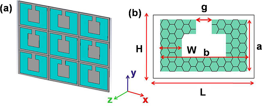
Figures 1(a) and 1(b) show the periodic devices arrangement and a single device of the graphene metamaterial, respectively. Graphene film was patterned to form an open square ring, as highlighted in the watchet area. The geometric parameters of the unit cell are (length) and (height). The unit SRR resonator consists of a graphene layer that has a length of (width of the square ring), (length of the square ring), and gap size . represents the line-width of the arm, and the LS layer is 105 nm. In order to obtain stronger resonances, we assume the thickness of graphene is 1 nm[10,11,17]. The permittivity of the LS is 2.25, which is mainly due to its weak dispersion and absorption[17]. CST Microwave Studio is used to calculate the electromagnetic response with a frequency domain solver. In the calculation, unit cell boundary conditions are set in both the X and Y directions, while the open boundary condition is set in the Z direction [Fig. 1(a)]. The THz transverse electromagnetic wave propagates in the minus Z direction with a linear polarization parallel to the direction of the gap-bearing side of the split ring. The parameter represents the transmission coefficients.
Sign up for Chinese Optics Letters TOC. Get the latest issue of Chinese Optics Letters delivered right to you!Sign up now
Figure 1.(a) Schematic of the SRR plasmonic structure. (b) A close-up picture of the patterned graphene metamaterial.
The conductivity of graphene consists of interband and intraband transition, which can be described by the formulas[6,11]where is the angular frequency, is the electron charge, is the reduced Planck constant, is the Boltzmann constant, is the temperature, is the Fermi level, which is the Fermi level value we used for the graphene referenced to the Dirac point. is the scattering coefficient[17], and is the velocity[17]. is the carrier mobility, which is decreased with an increasing carrier density (high Fermi level)[18,19], and it also can be demonstrated by the scattering coefficient. The value of the mobility ranges from 2000 to with graphene on the substrate at a high charge density, according to the experiment demonstration from Ref. [18]. When , the calculated mobility is , which can be achievable in the experiment[18,19]. In the THz region, intraband transition plays a dominant role rather than interband transition, which is prominent at the near infrared region. Here, the graphene optical conductivity can be illustrated by the Drude model. For , the conductivity can be expressed as follows[10]: Thus, the variation of the Fermi level can efficiently change the optical conductivity, which may further affect the electromagnetic response of our graphene metamaterial structure.
We investigate the influence of the Fermi level positions on the THz transmission. The THz transmission spectra of different Fermi levels are shown in Fig. 2(a), where the transmission dips corresponding to the plasmon resonances. The two resonance modes appear at approximately , and , respectively. The amplitude in the transmission spectra embodies the resonant strength. It can be seen that the transmission is close to 1 when the Fermi level is fixed to the Dirac point (i.e., ). For other cases of Fermi levels in the conduction band, the resonant strengths become pronounced. As shown in Fig. 2(a), the transmission of decreases from 0.58 to 0.28 when the Fermi level increases from 0.3 to 0.5 eV. Interestingly, the resonance frequency presents a blue-shift from 5.4 to 7.6 THz as the rising of the Fermi level. In this experiment, we mainly focus on the resonance frequency around and discuss the results at the Fermi level of 0.5 eV since it is comparative to the report in Ref. [10]. According to the formula[17]the carrier density is calculated to be , assuming . A higher carrier density allows for a stronger interaction between the incident THz wave and the graphene plasmonic metamaterial. As a result, a higher carrier density yields to both a stronger resonance strength and a larger resonance frequency.
Figure 2.(a) Transmission spectra of different Fermi levels and (b) surface current distribution of (7.6 THz) on the graphene metamaterial.
To further understand the mechanism of , we theoretically analyzed the current distribution of resonance frequency . The surface current of resonance frequency is shown in Fig. 2(b). In this case, the electric field is linearly polarized along the Y axis, which is unable to couple to the capacitance of the SRR or induce a circulating current. Thus, the case is not appropriate for forming a magnetic resonance (LC resonance)[20]. The current directions along the arms are parallel to each other, which indicate that it is an electric mode. The carriers along the two arms of the graphene metamaterial result in an enhanced dipolar coupling. The resonance strength of this electric mode (with a transmission of 0.28 at ) from our results is one of the strongest among some other reports.
From the above discussion, the resonance strength of the graphene metamaterial is strongly related to the width of the open square arms. Particularly, we investigate the influence of different arm-widths on the THz transmission and resonance. Figure 3(a) shows the transmission spectra of different arm line widths (0.6 to 1.4 μm) at 0.5 eV. The proposed design can be considered as an SRR with less than 1.55 μm. In the calculation, 1.4 μm is a proper value to analyze the device properties. The spectra unambiguously show that the transmission of frequency decreases from 0.48 to 0.15 when increases from 0.6 to 1.4 μm. Moreover, the resonant frequency blue-shifts from 5.2 to 9 THz with the increasing . With the increasing , the distance between the two arms is decreased, which can be regarded as two electric dipoles[9,21]. Therefore, the two dipoles are more repulsive, which leads to an enhanced restoring force that results in a higher resonance frequency[9,21]. Figure 3(b) shows the modulation depth as a function of frequency. The modulation depth can be defined as , where is the minimum transmission, while is the maximum transmission (0 eV). This monolayer patterned graphene metamaterial can achieve a peak modulation depth of 85% at . Here, we define an efficient modulation bandwidth when the modulation depth exceeds 50% (referring to the black dashed line). The modulation bandwidth is beyond 4 THz (7.5 to 11.5 THz) when . With changes from 1.4 to 0.6 μm, the modulation peak red-shifts to 3.5 THz and decreases by 33%, moreover, the modulation bandwidth is narrowed by 3.3 THz. On the one hand, with an increasing , the graphene area ratio in the unit cell increases, which leads to the increasing of absorption and reflection because of the more “metallic” graphene with a high Fermi level[22]. Meanwhile, the transmission is deeply suppressed, which contributes a lot to the increment of the modulation depth. On the other hand, the distance between two arms is shortened with the increasing arm-width, which also probably leads to the enhancement of the dipolar mode[21]. We can deduce that the modulation depth as well as the modulation bandwidth can be further enhanced via further increments in the arm-width (within 1.55 μm).
Figure 3.(a) Transmission spectra of different line-widths at 0.5 eV and (b) modulation depth () spectra.
In order to obtain more efficient THz modulation, we investigated the influence of stacked graphene plasmonic metamaterial layers on transmission and resonance. The parameters are the same as the aforementioned monolayer structure. Figure 4(a) shows the transmission spectra of the graphene metamaterial when the number of graphene layers varies from two to five. We observed two prominent features in Fig. 4(a). First, the resonance strength of becomes stronger, and the transmission of reduces (from 0.15 to 0.1) with more graphene layers. Second, the resonance frequency of the stacked layers for blue-shifted from 12.5 to 20 THz with layers changing from two to five. These phenomena in multiple graphene layers can be explained by the stronger Coulomb interaction of the adjacent layers[23]. The in-phase collective motion of carriers among the layers results in a stronger restoring force due to dipole-dipole coupling[2,23]. Since the thickness of a thin LS between each layer of graphene SRRs is 1 nm, which is much smaller than the unit cell, our simulation can nicely satisfy the strong coupling condition[22]. The carrier density of each graphene layer is identical, in this assumption, the carrier density of stacked graphene plasmonic layers can be regarded as times of the density in the original monolayer graphene, where is the number of graphene layers[2,23]. Figure 4(b) shows the modulation depth spectra of multiple graphene layers. The peak modulation depth of the five-layer graphene metamaterial approaches 99%, and the modulation bandwidth is 14.5 THz (13 to 27.5 THz). With the number of graphene layers increasing from one to five, the peak modulation depth changes from 85% to 99%, while the modulation bandwidth enlarges from 4 to 14.5 THz. It implies that by further increasing the graphene layers, the modulation depth and modulation bandwidth are able to be further improved.
Figure 4.(a) Transmission spectra of different layers at 0.5 eV and (b) modulation depth spectra.
The discussion from above is under the case of normal incidence, and in most practical applications, oblique incidence should also be considered. Figures 5(a) and 5(b) show the transmission and modulation depth spectra of the unit cell with a fixed value of as a function of incident angle . Two resonance modes were observed when is less than 30°, while for the those over 30°, three resonant modes appear at approximately , , and . Figures 5(c), 5(d), and 5(e) show the corresponding surface currents of the resonant modes when . is a magnetic mode with the circulating current induced by the acquiring component perpendicular to the SRR plane of the magnetic field via the induction law. and are of the higher-order modes. The resonance strength of becomes stronger (transmission reduces from 0.88 to 0.59) when the incidence angle increases, since the magnetic field acquires an increasing component[19]. The resonance strength of becomes stronger while becomes weaker with an increasing incident angle. The little shift of the resonant frequencies from all modes can be ignored. The peak modulation depth of 80% was obtained under an oblique incidence angle of . This modulation depth was then reduced to the lowest value of 54% at the incidence angle of . In addition, we also observed that there is a bandwidth of the modulation depth beyond 50% over all ranges of angles. The maximum modulation bandwidth is 3.8 THz at . In Fig. 5(b), the modulation depth of (lower frequency) is higher under a small incidence angle, while (higher frequency) presents an opposite result. This property reveals that our proposed graphene metamaterial suits low frequency THz wave modulation under small incidence angle and high frequency THz wave modulation under large incidence angles. Our monolayer graphene metamaterial design performs well in modulating the amplitude of the transmitted THz waves in oblique incidence conditions during a certain frequency region.
Figure 5.(a) and (b) THz wave transmission and modulation depth spectra as a function of frequency of different incidence angles. (c), (d), and (e) Surface current distributions of the three resonant modes.
In conclusion, we propose a graphene-based metamaterial to manipulate the optical response of a THz wave. It is revealed that the arm-width and graphene layers number on the metamaterial are two critical parameters to influence the THz wave modulation efficiency. High modulation depths of 85% and 80% are achieved in our monolayer graphene-based device under normal and oblique incidence, respectively. Further investigation reveals that the modulation depth can be enhanced to 99% by stacking five graphene layers in the metamaterial structure. Our results provide a new candidate for high efficiency manipulation of THz photonics and optoelectronics.