
Yang Ren, Vien Van, "Ultrawide-band silicon microring avalanche photodiode with linear photocurrent-wavelength response," Photonics Res. 9, 2303 (2021)
- Photonics Research
- Vol. 9, Issue 11, 2303 (2021)
Abstract
1. INTRODUCTION
With the advent of silicon (Si) photonics technology, there has been an increasing need for all-Si photodiodes (PDs) at the telecommunication wavelengths that are fully CMOS-compatible and can be monolithically integrated with other Si photonic components. As the bandgap wavelength of Si is around 1.1 μm, photodetection based on linear photon absorption in Si material at telecommunication wavelengths is very inefficient, thus necessitating the use of Ge-doped Si or Ge-on-Si PDs in most applications [1–3]. Si PDs based on two-photon absorption (TPA), on the other hand, do not require Ge, but these devices suffer from low responsivities and nonlinear current-optical power characteristics [4]. Photodetection in Si pin and pn junctions based on defect state absorption (DSA), where the defects are specially implanted [5–8] or comprise the same doping impurities (boron and phosphorus) available during the formation of diode junctions in the conventional CMOS process [9–12], can have good current-power linearity and high bandwidth operations similar to Ge–Si PDs. For example, Si pin diodes implanted with
In this paper, we report a Si microring-enhanced avalanche PD (MR APD) based on DSA with unique linear photocurrent-wavelength response spanning the full free spectral range (FSR) of the microring resonator. The device is based on a separate absorption and multiplication (SAM) APD
2. DESIGN OF Si MR APD
The Si MR APD consists of a
Sign up for Photonics Research TOC. Get the latest issue of Photonics Research delivered right to you!Sign up now
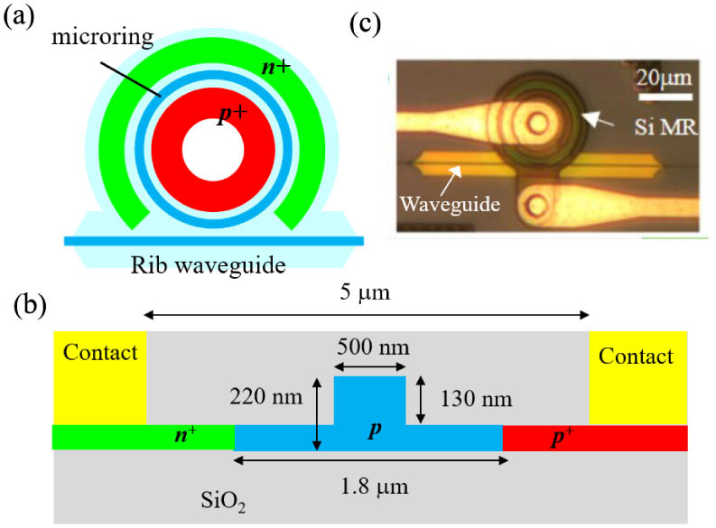
Figure 1.(a) Design of the MR APD and (b) schematic of the Si rib waveguide embedded with a
The
![]()
Figure 2.(a) Linear resonance transmission spectrum of the microring at 0 V bias (
As will be shown below, under illumination, the photocurrent of the MR APD depends on both the bias voltage and the optical power in the microring, so it is not straightforward to determine the multiplication factor of the MR APD due to impact ionization in the avalanche regime. We may, however, obtain an estimate of the multiplication factor from the dark current curve in Fig. 2(b). Taking the unity gain bias voltage as 10 V where the current begins to increase due to impact ionization, we estimate the multiplication factor of the MR APD to be about 16 times at an operating bias voltage of 15 V.
3. PERFORMANCE CHARACTERISTICS OF THE MR APD
The photodetection performance of the MR APD depends strongly on the resonance spectrum of light inside the microring resonator. For the MR APD, the resonance spectrum is significantly modified from the linear resonance spectrum in Fig. 2(a) due to strong optical nonlinearity induced by free carrier (FC) dispersion and the thermo-optic effect in the Si waveguide. We first measured the optical transmission response of the MR APD by coupling TE-polarized light from a tunable laser to the input waveguide. Figures 3(a) and 3(b) show the transmitted optical spectra swept over the 1522.2 nm resonance for different input optical powers
![]()
Figure 3.Optical transmission spectra of the MR APD near the 1522.2 nm resonance for increasing input optical powers at reverse bias voltage (a)
Also, from the minimum power transmission,
Figure 4(a) plots the total loss coefficient
![]()
Figure 4.(a) Plot of the total loss coefficient
The results in Fig. 4(c) indicate a giant thermo-optic nonlinear effect in the MR APD, which can cause the nonlinear phase to exceed
![]()
Figure 5.Variations of the photocurrent with wavelength of the MR APD at 15 V reverse bias voltage; black curve is the response at low input optical power (46 μW) multiplied by a factor of 10 to make it visible; red and green curves are the responses at high input optical power (1.86 mW) obtained from forward and reverse wavelength scans, respectively. The dotted line is the best linear fit to the forward photocurrent spectrum over the 1518.5–1522.5 nm wavelength range.
Another remarkable feature of the photocurrent spectrum in Fig. 5 is that the current varies linearly with the wavelength over the microring’s FSR, with a sensitivity slope of 0.576 mA/nm and linear correlation coefficient
For large
The large photogenerated currents also lead to very high responsivities for the MR APD at high reverse bias voltages near breakdown. In Fig. 6, we plot the peak responsivity, defined as
![]()
Figure 6.Peak responsivity and ratio of the peak photocurrent to dark current of the MR APD as functions of the input optical power at 13 and 15 V reverse bias voltages.
Although our MR APD was not optimized for high-speed operation, we also performed time-domain measurements to estimate the device’s time response to input optical pulses. We biased the MR APD at 15 V and applied an input optical signal of 1 mW power at 1523.2 nm wavelength (
![]()
Figure 7.Detected photocurrent waveform (converted to voltage) for a square-wave optical input signal of 1 MHz frequency; lower panels are the zoomed-in views of the rising and falling edges of the waveform.
4. DISCUSSION AND CONCLUSION
The unique linear photocurrent spectrum of the MR APD spanning the full FSR could enable many interesting applications, especially given the compact size of the device. Here we briefly propose three potential applications. As the first application, the MR APD may be used for wavelength-resolved photodetection as a compact on-chip spectrometer. For example, the device can be used to monitor or identify the wavelengths of optical signals in a wavelength division multiplexing network. Since the MR APD is sensitive to both the wavelength and optical power, a separate photodetector would be required to independently determine the power of the optical signal, which is then used along with the MR APD photocurrent to accurately determine its wavelength. Another application that takes advantage of the linear photocurrent spectrum of the MR APD is characterization of linear frequency chirped laser sources, such as those used in lidars. The conventional approach for measuring linear frequency chirp is to use a Mach–Zehnder interferometer and PDs [22,23]. Here the MR APD could offer a simpler and much more compact solution. Finally, the device can be used as a refractometric sensor by detecting the change in the photocurrent in response to a change in the effective index of the microring resonator in the presence of an analyte. Due to the very broad band of the photocurrent spectrum, such a sensor would not require a laser source with precise wavelength tuning as in conventional microring sensors [24,25].
To summarize, we demonstrated a fully CMOS-compatible Si photodetector using a
References
[1] M. Huang, P. Cai, S. Li, G. Hou, N. Zhang, T.-I. Su, C.-Y. Hong, D. Pan. 56 GHz waveguide Ge/Si avalanche photodiode. Optical Fiber Communications Conference and Exposition (OFC), 1-3(2018).
[2] C.-L. Hsin, S.-M. Wang, G.-Y. Chen, M.-H. Wu, C.-W. Huang, S.-C. Hsu, S.-C. Lo. Si/Ge/Si photodetector by rapid-melting-growth technique. IEEE Trans. Nanotechnol., 17, 607-610(2018).
[3] J. Cui, Z. Zhou. High-performance Ge-on-Si photodetector with optimized DBR location. Opt. Lett., 42, 5141-5144(2017).
[4] Y. Ren, V. Van. Enhanced small-signal responsivity in silicon microring photodetector based on two-photon absorption. IEEE J. Sel. Top. Quantum Electron., 26, 3800208(2020).
[5] J. Bradley, P. Jessop, A. Knights. Silicon waveguide-integrated optical power monitor with enhanced sensitivity at 1550 nm. Appl. Phys. Lett., 86, 241103(2005).
[6] J. J. Ackert, A. S. Karar, D. J. Paez, P. E. Jessop, J. C. Cartledge, A. P. Knights. 10 Gbps silicon waveguide-integrated infrared avalanche photodiode. Opt. Express, 21, 19530-19537(2013).
[7] M. W. Geis, S. J. Spector, M. E. Grein, J. U. Yoon, D. M. Lennon, T. M. Lyszczarz. Silicon waveguide infrared photodiodes with >35 GHz bandwidth and phototransistors with 50 A/W response. Opt. Express, 17, 5193-5204(2009).
[8] X. Mao, P. Han, L. Gao, Y. Mi, S. Hu, Y. Fan, C. Zhao, Q. Wang. Selenium-doped silicon-on-insulator waveguide photodetector with enhanced sensitivity at 1550 nm. IEEE Photon. Technol. Lett., 23, 1517-1519(2011).
[9] S. T. Fard, K. Murray, M. Caverley, V. Donzella, J. Flueckiger, S. M. Grist, E. Huante-Ceron, S. A. Schmidt, E. Kwok, N. A. F. Jaeger, A. P. Knights, L. Chrostowski. Silicon-on-insulator sensors using integrated resonance-enhanced defect-mediated photodetectors. Opt. Express, 22, 28517-28529(2014).
[10] R. R. Grote, K. Padmaraju, B. Souhan, J. B. Driscoll, K. Bergman, R. M. Osgood. 10 Gb/s error-free operation of all-silicon ion-implanted-waveguide photo diodes at 1.55 μm. IEEE Photon. Technol. Lett., 25, 67-70(2012).
[11] B. Desiatov, I. Goykhman, J. Shappir, U. Levy. Defect-assisted sub-bandgap avalanche photodetection in interleaved carrier-depletion silicon waveguide for telecom band. Appl. Phys. Lett., 104, 091105(2014).
[12] Y. Li, S. Feng, Y. Zhang, A. W. Poon. Sub-bandgap linear-absorption-based photodetectors in avalanche mode in PN-diode-integrated silicon microring resonators. Opt. Lett., 38, 5200-5203(2013).
[13] X. Li, Z. Li, X. Xiao, H. Xu, J. Yu, Y. Yu. 40 Gb/s all-silicon photodetector based on microring resonators. IEEE Photon. Technol. Lett., 27, 729-732(2015).
[14] K. Nisbida, K. Taguchi, Y. Matsumoto. InGaAsP heterostructure avalanche photodiodes with high avalanche gain. Appl. Phys. Lett., 35, 251-252(1979).
[15] B. Souhan, R. R. Grote, J. B. Driscoll, R. M. Osgood. Ion-implanted silicon-waveguide avalanche photodiode with separate absorption-multiplication region for C-band operation. Frontiers in Optics, FTu2A–5(2012).
[16] https://www.lumerical.com/products/mode/. https://www.lumerical.com/products/mode/
[17] R. Van Overstraeten, H. De Man. Measurement of the ionization rates in diffused silicon P-N junctions. Solid-State Electron., 13, 583-608(1970).
[18] W. Maes, K. De Meyer, R. Van Overstraeten. Impact ionization in silicon: a review and update. Solid-State Electron., 33, 705-718(1990).
[19] M. Dinu, F. Quochi, H. Garcia. Third-order nonlinearities in silicon at telecom wavelengths. Appl. Phys. Lett., 82, 2954-2956(2003).
[20] S. A. Srinivasan, M. Berciano, P. De Heyn, S. Lardenois, M. Pantouvaki, J. Van Campenhout. 27 GHz silicon-contacted waveguide-coupled Ge/Si avalanche photodiode. J. Lightwave Technol., 38, 3044-3050(2020).
[21] Z. Su, E. S. Hosseini, E. Timurdogan, J. Sun, M. Moresco, G. Leake, T. N. Adam, D. D. Coolbaugh, M. R. Watts. Whispering gallery germanium-on-silicon photodetector. Opt. Lett., 42, 2878-2881(2017).
[22] S. N. Zheng, J. Zou, H. Cai, J. Song, L. Chin, P. Liu, Z. Lin, D. Kwong, A. Liu. Microring resonator-assisted Fourier transform spectrometer with enhanced resolution and large bandwidth in single chip solution. Nat. Commun., 10, 2349(2019).
[23] J. Yang, T. Yang, Z. Wang, D. Jia, C. Ge. A novel method of measuring instantaneous frequency of an ultrafast frequency modulated continuous-wave laser. Sensors, 20, 3834(2020).
[24] G. Mi, C. Horvath, M. Aktary, V. Van. Silicon microring refractometric sensor for atmospheric CO2 gas monitoring. Opt. Express, 24, 1773-1780(2016).
[25] W. Huang, Y. Luo, W. Zhang, C. Li, L. Li, Z. Yang, P. Xu. High-sensitivity refractive index sensor based on Ge–Sb–Se chalcogenide microring resonator. Infrared Phys. Technol., 116, 103792(2021).


Set citation alerts for the article
Please enter your email address

© Copyright 2018-2021 | Chinese Laser Press. All Rights Reserved 沪ICP备15018463号-20