Abstract
Metamaterials have demonstrated exotic electromagnetic properties, which offer a good platform for realizing light absorption, photodetection, filtering, and so on. However, broadband multifunctional metamaterial absorbers are restricted in cascaded structures. Here, broadband multifunctional properties were realized by introducing vanadium dioxide into a metamaterial absorber. Through the modified design and highly efficient utilization of multiple resonant modes, both plasmonic tunable color filters and near-infrared photodetectors can be simultaneously achieved by this construction. Meanwhile, active color and a photodetection band in the near-infrared range can become tunable with the insulating–metallic transition of vanadium dioxide. Thus, the variations of rendering colors could correspondingly indicate shifts of the near-infrared photodetection bands. This method theoretically confirms the feasibility of designing multifunctional devices via a vanadium-dioxide-based metamaterial absorber, which holds great promise for future versatile utilization of multiple physical mechanisms to achieve numerous functionalities in a simple nanostructure or device.1. INTRODUCTION
Metamaterials, artificial composite materials or structures, exhibit salient advantages in terms of controlling and manipulating light–matter interactions at subwavelength scale [1,2]. Therefore, they enable spectral engineering, phase manipulation, polarization control, such as light harvesting [3,4], filtering [5,6], modulation [7], optical angular momentum generation [8,9], holograms [10], polarization conversion [11,12], and many more processes. In general, particular spectral properties in such artificial engineered metamaterials emerge from optical resonances induced by composite nanostructures. Therefore, spectral information strongly relies on the size, shape, and arrangement of metallic or dielectric nanostructures. Most importantly, tailoring all parameters provides an efficient means for spectral management and therefore reaps significant benefits for achieving tunable spectra, especially in the visible range [13–15]. However, it will also be stuck in the fixed morphological nanostructure. With respect to this limitation, integrating or embedding the materials or structures with tunable optical properties could be a better approach to overcome the bottleneck [7,16–18].
So far, most research efforts in the visible range have been exerted on tunable structural colors via microelectromechanical systems (MEMS) [19], photonic crystals [20], mechanical deformation strategies [18,21], optoelectronic or electrochemical methods [22–24], etc. MEMS offer an avenue to form a gap changing Fabry–Perot (FP) cavity, which can produce a continuously varying color in the whole visible range. However, it is unfavorable for optoelectronic integration due to the complex control system. Photonic crystals can also provide a dynamically tunable capability of resonant wavelengths, i.e., colors, with the changes of effective refractive indices in the photonic crystal structures. Mechanical deformation strategies could support the changes of structural periods, which will produce dynamically tunable colors due to the changing of effective refractive index. In addition, optoelectronic methods can also tune the permittivity of materials such as transparent conductive oxides and graphene. Alternatively, electrochemical methods can afford the deposition or dissolution of noble metals, which directly alters morphological nanostructures, such as size and volume. Therefore, it will cause shifts of the resonant wavelengths, which can be regarded as the changing of colors in the visible frequency. Nevertheless, these strategies for changing colors, possessing both reversible dynamic response and distinct optical behavior, are naturally single function, which means that these structures or devices will work only in the visible spectral range for color filtering, color printing, sensing, and so on. While the rendering colors of the designed devices can represent the working state in the other spectra, like a pH indicator, it will therefore enhance efficiency and cost effectiveness. Phase-change materials exhibit broadband electromagnetic response with tunable properties, such as germanium-antimony-tellurium alloys () [25–28], and vanadium dioxide () [29], which could be excellent candidates for multiband and multifunctional applications. , an iconic example of a correlated electron material, has received significant attention because of its insulating–metallic transition (IMT) at [30,31]. In addition, the phase change due to a Mott transition in can directly change its refractive index, which has been proved by applying temperature [32,33], electrical fields [34], or light [33,35] in the visible, infrared, and other spectral regions [29,32,35,36]. However, most of functional devices based on work in a relatively narrow band, for example, it may work only as an infrared photodetector at 10.6 μm [37].
In this study, we introduce into the metal–insulator–metal (MIM) metamaterial absorber to create dynamic color display and near-infrared multiband photodetection. The property of freely designed working wavelength in the metamaterial absorber can realize near-infrared photodetection due to the hot-electron and photocarriers generated in the plasmonic structures based on the metasurface wave (M-wave) assisted absorption [38], while the collective utilization of other physical mechanisms can support the shorter resonant wavelengths, such as selective color filtering. The finite-difference time-domain (FDTD) method is used to simulate the light transmission behavior. Parametric investigation of the dynamically tunable colors and shifts of the photodetection bands in the near-infrared range is obtained. When the phase state of transits from the insulating state to the metallic state, the active color and near-infrared photodetection band will be changed at the same time. Therefore, the variations of rendering colors could correspondingly indicate the shifts of the working band in the near-infrared range.
Sign up for Photonics Research TOC. Get the latest issue of Photonics Research delivered right to you!Sign up now
2. DESIGN AND MODELING
The schematic of a multifunctional -based metamaterial absorber is shown in Fig. 1, where two-dimensional metal square nanoparticles are separated from the continuous metal film by a stack that includes an insulator layer and a film. Three-dimensional FDTD simulations (FDTD Solutions, Lumerical Solutions, Inc.) of a unit cell are performed with periodic boundary conditions in the plane, and perfectly matching layers are added in the direction to avoid interface reflection. In all simulations, the dimensions of mesh grids used are set as . The expected nanostructure is insensitive to light polarization due to symmetry in the plane. Herein, the incident light is assumed to be transverse magnetic (TM) polarized (the electric field along direction) and normal to the metamaterial absorber surface. is the identical period of a unit functional metamaterial structure along the and directions. Filling factor FF is the duty ratio of the nanoparticles. The thickness of the silver nanoparticles is globally set as 70 nm to make further fabrication easier. and are the thickness of the insulator and the film, respectively. Moreover, the thickness of the silver film on the bottom is more than 100 nm to act as a reflective mirror. The refractive index of the insulator is 2.0. Silver is used as the metal material with its dielectric constant from the data of Palik [39]. The optical constants of at the insulating state and the metallic state are extracted from Ref. [32].
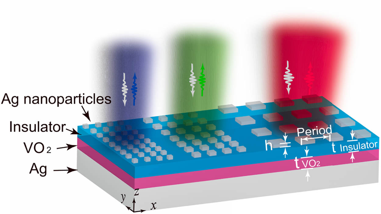
Figure 1.Schematic of the -based metamaterial photodetector with active color rendering.
3. RESULTS AND DISCUSSION
Figure 2(a) shows the calculated spectra with the phase transitions of at , , period , and filling factor . It can be clearly seen that the spectrum has changed significantly. The resonant wavelength shifts from 1467 to 1928 nm in the near-infrared range. When the period decreases from 470 to 440 nm and the filling factor becomes 0.5, as shown in Fig. 2(b), the resonant wavelength in the near-infrared shifts from 2224 to 3016 nm. When the period and filling factor FF are, respectively, 260 nm and 0.6, the resonant wavelength in the near-infrared also varies from 1686 to 2213 nm with phase transition, as observed in Fig. 2(c). These results confirm the initial resonant wavelength shift toward the longer wavelength with phase transition of , where the shifting of resonant wavelengths could support multiband photodetection. Moreover, the changes of the reflection at the initial resonant wavelength provide the switching state. Meanwhile, differences of the spectra between the insulating state and the metallic state have also occurred in the visible regime. To further investigate the differences of the spectra between the two states in the visible frequency range, the chromaticity is calculated by interpreting the reflective spectrum with respect to the color-matching functions of the human eye as defined by the International Commission on Illumination (Commission Internationale de l’Eclairage, CIE) [40,41]. The data in the CIE chromaticity diagram can intuitively represent the variations of the structural colors. As shown in Fig. 2(d), the red squares stand for the corresponding colors of the reflective spectra in Figs. 2(a)–2(c) at the insulating state of , while the blue circular dots represent those at the metallic state. Thus, the square dots can be regarded as the vertices of a triangle that shows the color gamut when is at the insulating state, while the blue triangle with the blue circular dots represents the color space at the metallic state. It can be clearly seen that color has changed dramatically with phase transition; for example, the color shifts from green to aquamarine at period and filling factor . In addition, the associated rendering colors of the spectra under D65 illumination (North daylight illuminant) are depicted in the inset. It, therefore, confirms the color changes with phase transition. As a consequence, when the phase transition occurs, the resonant wavelength at the near-infrared range and the spectrum in the visible frequency (or color) range will simultaneously change, which can be identified as an appreciable synergetic relationship between the photodetection band in the near-infrared and the actively rendering color. Moreover, the slight variations of the colors can directly indicate significant shifts of the photodetection band in the near-infrared range. Also, the initial and subsequent bands of photodetection with the insulating–metallic transition jointly contribute to broadband photodetection in the near-infrared range.

Figure 2.Calculated reflection spectra of the -based metamaterial absorber with phase transitions from the insulating state to the metallic state at , , (a) , , (b) , , and (c) , . The solid line represents the reflective spectrum at the insulating state, while the dashed line stands for the spectrum at the metallic state. (d) The calculated CIE 1931 chromaticity diagram of the corresponding spectra showing in (a)–(c). The red triangle formed by the red squares as the triangle vertices shows the color gamut when is at the insulating state, while the blue triangle formed by the blue circles represents the color space at the metallic state.
To investigate the physical mechanism of the multifunctional -based metamaterial absorber, the reflection characteristics of the proposed structure are scrutinized with various periods, and the filling factor FF, , and are fixed at 0.5, 20 nm, and 5 nm, respectively. Figure 3(a) shows the calculated reflection spectra at both the insulating and metallic states with the period ranging from 220 to 700 nm in increments of 40 nm. The optical responses manifest a substantially lower reflection at particular wavelengths according to the periods of the nanoparticles, following four trends indicated by the dashed lines marked A, B, C, and D from the shorter wavelengths to the longer ones. These dashed lines can be clearly seen in the contour maps of the reflection spectra with more detailed data, which are normalized to the area of the unit cell at the insulating state and the metallic state of the film, respectively, as shown in Figs. 3(b) and 3(c). Lines A (cyan dashed line), B (white dashed line), and C (magenta dashed line) collectively dominate the spectra in the visible range, i.e., rendering colors, while line D (yellow dashed line) in the near-infrared range possesses low reflection, which means high absorption in the proposed metamaterial structures may support high efficiency photodetection. Moreover, compared to line D in Figs. 3(b) and 3(c), photodetection bands have significant changes. Therefore, owing to the insulating–metallic transition, multiband photodetection can be achieved in the -based metamaterial absorbers with simultaneous color rendering.
Figure 3.(a) Reflection spectra of the -based metamaterial absorbers at the insulating and metallic states when the period varies from 220 to 700 nm, with the dashed trend lines tracing the location of similar resonant modes. Filling factor FF, , and are fixed at 0.5, 20 nm, and 5 nm, respectively. (b), (c) Contour maps of the reflection spectra in (a) that are normalized to the area of the unit cell with the insulating and metallic states, respectively.
To further explore the origins of lines A–D, we analyze the impact of geometric transformation using a straightforward and physically intuitive procedure with the insulating state of . In these simulations, periods in both the and directions are fixed to 500 nm and FF yields to be 0.5 in either the or direction. Moreover, the polarization of the illumination light is along the direction, and the rest of the parameters are the same as those of the insulating state in Fig. 3(a). As a comparison, the structure with no silver nanoparticles has also been calculated as the blank control group. As shown in Fig. 4(a), FF in the direction is fixed at 0.5, while it varies from 0.3 to 0.7 in the direction. However, the FFs in the and directions presented in Fig. 4(b) are opposite to those in Fig. 4(a). The first dip bands are all around 435 nm in both Figs. 4(a) and 4(b). Compared to the reflective spectrum with no nanoparticles shown in the dotted line, the entire resonant wavelengths of this mode have slight blueshifts owing to the coupling of the transverse propagation surface plasmon polariton (SPP) modes. Therefore, this mode, line A in Fig. 3(a), may be attributed to the longitudinal FP cavity modes supported by the cavity. The second dips around 500 nm in both Figs. 4(a) and 4(b) do not change when the structure changes, with the resonant wavelength equal to the period. In addition, these dips shift from 380 to 700 nm in a linear manner, shown as line B in Fig. 3(a), with the period varying from 380 to 700 nm. This is accounted for by Wood’s anomaly for the Ag–air interface, as in the case of diffraction gratings. The wavelength can be dictated by the equation , where is the wavelength, is the period, is the permittivity of the dielectric at the interface, and and are integers signifying the order of resonance. Compared to the first dips around 435 nm, there are significant differences at the third dips [denoted as line C in Fig. 3(a)] between the increasing filling factors in the and directions in Figs. 4(a) and 4(b). As shown in Fig. 4(a), the third dips shift from 557 to 713 nm with FF ranging from 0.3 to 0.7. However, it varies only from 647 to 683 nm in Fig. 4(b). That means the shifting of the resonant wavelength is mainly associated with the geometry of the nanoparticles along the polarization direction. Therefore, we regard this mode as the transverse FP cavity modes [42]. In addition, as demonstrated in the insets of Figs. 4(a) and 4(b), the fourth resonant wavelengths [line D in Fig. 3(a)] in the near-infrared range have behavior similar to that of the third ones, either at the insulating state or the metallic state. The longitudinal FP cavity mode () and localized SPP mode in the MIM metamaterial structure dominate this so-called metamaterial gap plasmon phenomenon [43].
Figure 4.Calculated reflection spectra with different filling factors ranging from 0.3 to 0.7 in the (a) and (b) directions at the insulating state with the associated filling factor in the and directions. , , and are fixed at 500, 20, and 5 nm, respectively. “None” means there is no silver nanoparticle in the structure. The normal polarization illumination light is along the direction. (c)–(e) The magnetic field distributions at resonant wavelengths of 440, 665, and 2500 nm with period , respectively. The filling factor FF in both the and directions is fixed at 0.5. The rest of the parameters are the same as the insulating ones in Fig. 3(a).
By exploring the optical response with variable filling factors at insulating state with period , we preliminarily elucidate the core physical mechanisms underlying the selective spectra dips in reflection. To scrutinize the relative modes or phenomena, we plot the magnetic field distribution at the resonant wavelengths of lines A, C, and D with period and filling factor in both the and directions. The other parameters are the same as the insulating ones in Fig. 3(a). As shown in Fig. 4(c), the field distribution at wavelength of 440 nm exhibits a legible feature of a longitudinal FP cavity mode as the higher field intensity located at the -film–Ag mirror interface. Meanwhile, the SPPs excited at the sidewalls (Ag–air interface) of the nanoparticles exhibit a weak coupling with the FP cavity mode. Thus, the longitudinal FP cavity mode and the SPP mode act collectively to inhibit the reflection around specific wavelengths, marked as line A. Alternatively, the SPPs excited at the backside of the nanoparticles (Ag–insulator interface) carry the coupling electromagnetic power and propagate transversely, forming a transverse FP resonator, as illustrated in Fig. 4(d). The field distribution at wavelength of 650 nm (denoted as line C) locates mainly in the dielectric layers between the upper and lower metal layers where the field maximum tends to be concentrated in the center area of the slits, which is coincident with the transverse FP mode. As presented in Fig. 4(e), the field profile at resonant wavelength at 2500 nm (denoted as line D) shows a standard FP mode in the MIM metamaterial structure. The expected metamaterial absorber can be regarded as a combination of a microcavity and surface plasmonic structures, where both the surface plasmon resonances near field enhancement and light recycling contribute to the high light absorption shown in Fig. 3. Thus, hot-electron photodetection with the plasmonic structures and photodetection with the -based cavity photodetector jointly contribute to the total photodetection of the -based metamaterial absorber.
Having analyzed the physical mechanisms in the proposed metamaterial absorber, we build a database of reflection spectra in the visible and near-infrared ranges with different periods and filling factors at the insulating state and the metallic state. Although the CIE chromaticity could present the spectra, it cannot demonstrate the real colors as we see in the natural world. To get a better understanding of the actual colors, the corresponding colors of the spectra under D65 illumination are depicted in Fig. 5. Responses have been achieved in nearly the entire visible range with variable geometric parameters at both the insulating and metallic states when the period varies from 260 to 580 nm, and the filling factor changes from 0.3 to 0.6. In addition, colors with the same geometric parameters have changed with the phase transition, so are the photodetection bands in the near-infrared range. For example, the color shifts from green to aquamarine and the photodetection band in the near-infrared range changes from 2224 to 3016 nm with the phase transition at period and filling factor . Consequently, slight changes of color can predict significant changes of photodetection bands. Thus, we can roughly deduce the photodetection band from the rendering color rather than from an additional spectrometer and thermometer.
Figure 5.Calculated colors evolve with different periods and filling factors at the insulating state and the metallic state under D65 illuminations. The period varies from 260 to 580 nm, and the filling factor changes from 0.3 to 0.6.
4. CONCLUSIONS
In summary, a unique strategy for multifunctional devices is proposed to achieve active color rendering and multiband photodetection in a -based metamaterial absorber. Through the modified design and highly efficient utilization of multiple resonant modes in the -based metamaterial absorber, both plasmonic tunable color filters and near-infrared photodetectors can be simultaneously achieved, and the filtering colors and photodetection bands will change with the phase transition. Moreover, the slight variations of rendering colors can correspondingly indicate remarkable shifts of bands of photodetection in the near-infrared range. The appreciable synergetic relationship between the photodetection bands in the near-infrared and active rendering colors reveals the feasibility of utilizing -based metamaterial absorbers, rather than the cascaded structures, for designing multifunctional devices, which may shed some light on expanding the utilization of multiple physical mechanisms to achieve versatile functionalities in a simple nanostructure or device.
References
[1] D. R. Smith, J. B. Pendry, M. C. K. Wiltshire. Metamaterials and negative refractive index. Science, 305, 788-792(2004).
[2] N. I. Landy, S. Sajuyigbe, J. J. Mock, D. R. Smith, W. J. Padilla. Perfect metamaterial absorber. Phys. Rev. Lett., 100, 207402(2008).
[3] C. M. Watts, X. L. Liu, W. J. Padilla. Metamaterial electromagnetic wave absorbers. Adv. Mater., 24, 98-120(2012).
[4] L. Wen, Y. F. Chen, W. W. Liu, Q. Su, J. Grant, Z. Y. Qi, Q. L. Wang, Q. Chen. Enhanced photoelectric and photothermal responses on silicon platform by plasmonic absorber and Omni-Schottky junction. Laser Photon. Rev., 11, 1700059(2017).
[5] T. Xu, Y. K. Wu, X. G. Luo, L. J. Guo. Plasmonic nanoresonators for high-resolution colour filtering and spectral imaging. Nat. Commun., 1, 59(2010).
[6] Q. Chen, D. R. S. Cumming. High transmission and low color cross-talk plasmonic color filters using triangular-lattice hole arrays in aluminum films. Opt. Express, 18, 14056-14062(2010).
[7] Y. W. Huang, H. W. H. Lee, R. Sokhoyan, R. A. Pala, K. Thyagarajan, S. Han, D. P. Tsai, H. A. Atwater. Gate-tunable conducting oxide metasurfaces. Nano Lett., 16, 5319-5325(2016).
[8] M. Pu, X. Li, X. Ma, Y. Wang, Z. Zhao, C. Wang, C. Hu, P. Gao, C. Huang, H. Ren, X. Li, F. Qin, J. Yang, M. Gu, M. Hong, X. Luo. Catenary optics for achromatic generation of perfect optical angular momentum. Sci. Adv., 1, e1500396(2015).
[9] Y. H. Guo, M. B. Pu, Z. Y. Zhao, Y. Q. Wang, J. J. Jin, P. Gao, X. Li, X. L. Ma, X. G. Luo. Merging geometric phase and plasmon retardation phase in continuously shaped metasurfaces for arbitrary orbital angular momentum generation. ACS Photon., 3, 2022-2029(2016).
[10] X. Li, L. Chen, Y. Li, X. Zhang, M. Pu, Z. Zhao, X. Ma, Y. Wang, M. Hong, X. Luo. Multicolor 3D meta-holography by broadband plasmonic modulation. Sci. Adv., 2, e1601102(2016).
[11] X. L. Ma, C. Huang, M. B. Pu, Y. Q. Wang, Z. Y. Zhao, C. T. Wang, X. G. Luo. Dual-band asymmetry chiral metamaterial based on planar spiral structure. Appl. Phys. Lett., 101, 161901(2012).
[12] X. L. Ma, W. B. Pan, C. Huang, M. B. Pu, Y. Q. Wang, B. Zhao, J. H. Cui, C. T. Wang, X. G. Luo. An active metamaterial for polarization manipulating. Adv. Opt. Mater., 2, 945-949(2014).
[13] V. R. Shrestha, S. S. Lee, E. S. Kim, D. Y. Choi. Aluminum plasmonics based highly transmissive polarization-independent subtractive color filters exploiting a nanopatch array. Nano Lett., 14, 6672-6678(2014).
[14] X. M. Goh, Y. H. Zheng, S. J. Tan, L. Zhang, K. Kumar, C. W. Qiu, J. K. W. Yang. Three-dimensional plasmonic stereoscopic prints in full colour. Nat. Commun., 5, 5361(2014).
[15] N. S. King, L. F. Liu, X. Yang, B. Cerjan, H. O. Everitt, P. Nordlander, N. J. Halas. Fano resonant aluminum nanoclusters for plasmonic colorimetric sensing. ACS Nano, 9, 10628-10636(2015).
[16] S. H. Lee, M. Choi, T. T. Kim, S. Lee, M. Liu, X. Yin, H. K. Choi, S. S. Lee, C. G. Choi, S. Y. Choi, X. Zhang, B. Min. Switching terahertz waves with gate-controlled active graphene metamaterials. Nat. Mater., 11, 936-941(2012).
[17] X. Y. Duan, S. Kamin, N. Liu. Dynamic plasmonic colour display. Nat. Commun., 8, 14606(2017).
[18] S. C. Song, X. L. Ma, M. B. Pu, X. Li, K. P. Liu, P. Gao, Z. Y. Zhao, Y. Q. Wang, C. T. Wang, X. G. Luo. Actively tunable structural color rendering with tensile substrate. Adv. Opt. Mater., 5, 1600829(2017).
[19] J. Hong, E. Chan, T. Chang, T. C. Fung, B. Hong, C. Kim, J. Ma, Y. L. Pan, R. Van Lier, S. G. Wang, B. Wen, L. X. Zhou. Continuous color reflective displays using interferometric absorption. Optica, 2, 589-597(2015).
[20] H. Wang, K. Q. Zhang. Photonic crystal structures with tunable structure color as colorimetric sensors. Sensors, 13, 4192-4213(2013).
[21] M. L. Tseng, J. Yang, M. Semmlinger, C. Zhang, P. Nordlander, N. J. Halas. Two-dimensional active tuning of an aluminum plasmonic array for full-spectrum response. Nano Lett., 17, 6034-6039(2017).
[22] A. C. Arsenault, T. J. Clark, G. Von Freymann, L. Cademartiri, R. Sapienza, J. Bertolotti, E. Vekris, S. Wong, V. Kitaev, I. Manners, R. Z. Wang, S. John, D. Wiersma, G. A. Ozin. From colour fingerprinting to the control of photoluminescence in elastic photonic crystals. Nat. Mater., 5, 179-184(2006).
[23] F. Lutolf, O. J. F. Martin, B. Gallinet. Fano-resonant aluminum and gold nanostructures created with a tunable, up-scalable process. Nanoscale, 7, 18179-18187(2015).
[24] G. P. Wang, X. C. Chen, S. Liu, C. P. Wong, S. Chu. Mechanical chameleon through dynamic real time-plasmonic tuning. ACS Nano, 10, 1788-1794(2016).
[25] M. A. Kats, R. Blanchard, P. Genevet, F. Capasso. Nanometre optical coatings based on strong interference effects in highly absorbing media. Nat. Mater., 12, 20-24(2013).
[26] P. Hosseini, C. D. Wright, H. Bhaskaran. An optoelectronic framework enabled by low-dimensional phase-change films. Nature, 511, 206-211(2014).
[27] Y. G. Chen, X. Li, X. G. Luo, S. A. Maier, M. H. Hong. Tunable near-infrared plasmonic perfect absorber based on phase-change materials. Photon. Res., 3, 54-57(2015).
[28] G. Bakan, S. Ayas, T. Saidzoda, K. Celebi, A. Dana. Ultrathin phase-change coatings on metals for electrothermally tunable colors. Appl. Phys. Lett., 109, 071109(2016).
[29] S. Kumar, J. P. Strachan, A. L. D. Kilcoyne, T. Tyliszczak, M. D. Pickett, C. Santori, G. Gibson, R. S. Williams. The phase transition in VO2 probed using X-ray, visible and infrared radiations. Appl. Phys. Lett., 108, 073102(2016).
[30] S. D. Ha, Y. Zhou, A. E. Duwel, D. W. White, S. Ramanathan. Quick switch: strongly correlated electronic phase transition systems for cutting-edge microwave devices. IEEE Microw. Mag., 15, 32-44(2014).
[31] S. Y. Zhang, M. A. Kats, Y. J. Cui, Y. Zhou, Y. Yao, S. Ramanathan, F. Capasso. Current-modulated optical properties of vanadium dioxide thin films in the phase transition region. Appl. Phys. Lett., 105, 211104(2014).
[32] M. J. Dicken, K. Aydin, I. M. Pryce, L. A. Sweatlock, E. M. Boyd, S. Walavalkar, J. Ma, H. A. Atwater. Frequency tunable near-infrared metamaterials based on VO2 phase transition. Opt. Express, 17, 18330-18339(2009).
[33] J. D. Ryckman, V. Diez-Blanco, J. Nag, R. E. Marvel, B. K. Choi, R. F. Haglund, S. M. Weiss. Photothermal optical modulation of ultra-compact hybrid Si-VO2 ring resonators. Opt. Express, 20, 13215-13225(2012).
[34] M. D. Goldflam, M. K. Liu, B. C. Chapler, H. T. Stinson, A. J. Sternbach, A. S. McLeod, J. D. Zhang, K. Geng, M. Royal, B. J. Kim, R. D. Averitt, N. M. Jokerst, D. R. Smith, H. T. Kim, D. N. Basov. Voltage switching of a VO2 memory metasurface using ionic gel. Appl. Phys. Lett., 105, 041117(2014).
[35] Z. J. Thompson, A. Stickel, Y. G. Jeong, S. Han, B. H. Son, M. J. Paul, B. Lee, A. Mousavian, G. Seo, H. T. Kim, Y. S. Lee, D. S. Kim. Terahertz-triggered phase transition and hysteresis narrowing in a nanoantenna patterned vanadium dioxide film. Nano Lett., 15, 5893-5898(2015).
[36] D. C. Wang, L. C. Zhang, Y. D. Gong, L. K. Jian, T. Venkatesan, C. W. Qiu, M. H. Hong. Multiband switchable terahertz quarter-wave plates via phase-change metasurfaces. IEEE Photon. J., 8, 5500308(2016).
[37] S. H. Chen, H. Ma, X. J. Yi, T. Xiong, H. C. Wang, C. J. Ke. Smart VO2 thin film for protection of sensitive infrared detectors from strong laser radiation. Sens. Actuators A Phys., 115, 28-31(2004).
[38] X. G. Luo. Principles of electromagnetic waves in metasurfaces. Sci. China Phys. Mech. Astron., 58, 594201(2015).
[39] E. D. Palik. Handbook of Optical Constants of Solids(1985).
[40] S. Westland, C. Ripamonti, V. Cheung. Computational Colour Science Using MATLAB(2012).
[41] T. Smith, J. Guild. The C.I.E. colorimetric standards and their use. Trans. Opt. Soc., 33, 73-134(1931).
[42] L. Wen, F. H. Sun, Q. Chen. Cascading metallic gratings for broadband absorption enhancement in ultrathin plasmonic solar cells. Appl. Phys. Lett., 104, 151106(2014).
[43] M. G. Nielsen, A. Pors, O. Albrektsen, S. I. Bozhevolnyi. Efficient absorption of visible radiation by gap plasmon resonators. Opt. Express, 20, 13311-13319(2012).

