
Yun-Tuan Fang, Zhang-Xin Wang, Er-Pan Fan, Xiao-Xue Li, Hong-Jin Wang. Topological phase transition based on structure reversal of two-dimensional photonic crystals and construction of topological edge states [J]. Acta Physica Sinica, 2020, 69(18): 184101-1
- Acta Physica Sinica
- Vol. 69, Issue 18, 184101-1 (2020)
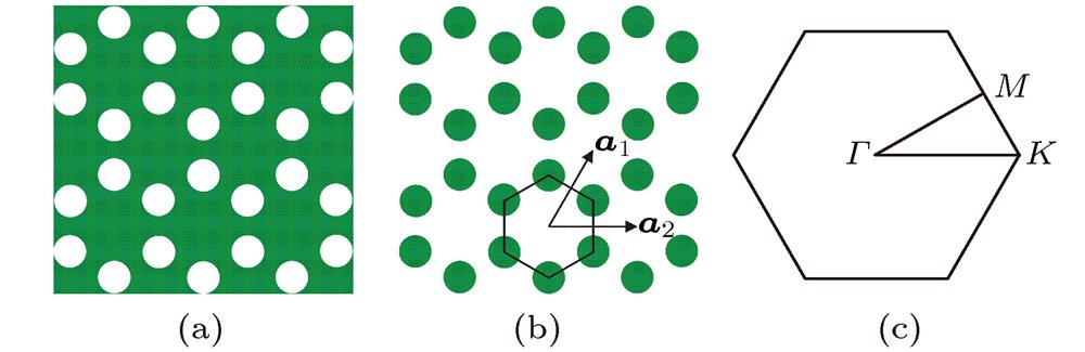
Fig. 1. Schematic of hexagonal honeycomb lattice (the hexagon is the unit cell, and a 1 and a 2 are the basic vectors of lattice): (a) The scatterer and matrix are air rods and dielectric, respectively; (b) the scatterer and matrix are dielectric rods and air, respectively; (c) the first Brillouin zone.
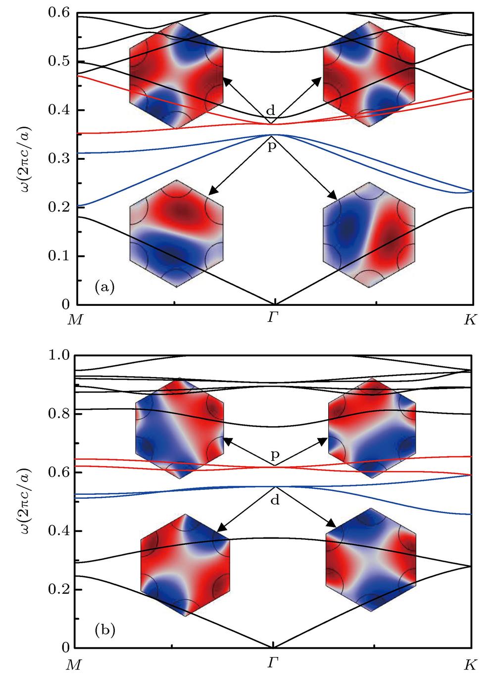
Fig. 2. Band structures of the hexagonal honeycomb lattices, and the orbitals of p and d: (a) Type A; (b) type D.
Fig. 3. Frequency positions of p and d orbits with the differences of
 and
and

and
Fig. 4. Band structures of the optimized lattices, and the orbitals of p and d: (a) Type A; (b) type D.
Fig. 5. Construction and analysis of the edge states: (a) Supercell; (b) bands of the supercell; (c) mode analysis. The mode field E z of the energy flow vectors of points A and B in (c) reveal the pseudo spins at the two edges of the middle non-trivial layer in (a). Because the energy flow vectors at the edge are much larger than those in the vortex, we move the vector plots to the non-trivial layer for a proper distance.
Fig. 6. Edge state transmission of electromagnetic wave excited by pseudospin source (white hexagon star): (a) Frequency position at AB and counterclockwise spin; (b) frequency position at AB and clockwise spin; (c) frequency position at CD and counterclockwise spin; (d) frequency position at CD and clockwise spin.
Fig. 7. Robust of the topological boundary states and the pseudo-spin source position represented by white hexagonal star: (a) The distribution of the E z field amplitude with the obstacle (the black area in the illustration) permittivity 2.25; (b) the distribution of the E z field amplitude with the obstacle permittivity 11.7; (c) the distribution of the E z field from the edge state transmission along the z-type route (the inset shows a locally amplified Poynting vector distribution); (d) the distribution of the E z field and the energy flow vectors from the edge state transmission along the z-type route with the source moved 3a to the right.
|
Table 1. Distribution of electric field energy density in two structures.

Set citation alerts for the article
Please enter your email address
© Copyright 2018-2021 | Chinese Laser Press. All Rights Reserved 沪ICP备15018463号-20