Tianjiang He, Suping Liu, Wei Li, Li Zhong, Xiaoyu Ma, Cong Xiong, Nan Lin, Zhennuo Wang. Study of quantum well mixing induced by impurity-free vacancy in the primary epitaxial wafers of a 915 nm semiconductor laser[J]. Journal of Semiconductors, 2023, 44(10): 102302
Copy Citation Text
Output power and reliability are the most important characteristic parameters of semiconductor lasers. However, catastrophic optical damage (COD), which usually occurs on the cavity surface, will seriously damage the further improvement of the output power and affect the reliability. To improve the anti-optical disaster ability of the cavity surface, a non-absorption window (NAW) is adopted for the 915 nm InGaAsP/GaAsP single-quantum well semiconductor laser using quantum well mixing (QWI) induced by impurity-free vacancy. Both the principle and the process of point defect diffusion are described in detail in this paper. We also studied the effects of annealing temperature, annealing time, and the thickness of SiO2 film on the quantum well mixing in a semiconductor laser with a primary epitaxial structure, which is distinct from the previous structures. We found that when compared with the complete epitaxial structure, the blue shift of the semiconductor laser with the primary epitaxial structure is larger under the same conditions. To obtain the appropriate blue shift window, the primary epitaxial structure can use a lower annealing temperature and shorter annealing time. In addition, the process is less expensive. We also provide references for upcoming device fabrication.
The 915/975 nm semiconductor lasers play an important role in pump sources, medical devices, chemical production, and optical communication thanks to their small size, light weight, and high power[1]. However, due to the characteristics of semiconductor lasers, the output power at the output cavity surface is the largest. In addition, there are a lot of surface states and defects at the cavity surface because of dissociation, which result in numerous non-radiative recombination centers and promote the temperature rise at the cavity surface. The increase of temperature will narrow the band gap at the cavity surface, resulting in numerous non-radiation recombinations and leading reactions on the cavity surface to form a positive feedback process. Finally, the cavity surface will melt due to the optical power density overload at the cavity surface will melt due to the optical power density overload at the cavity surface. The COD can be refrained by using QWI to prepare NAW at the cavity surface to reduce photon absorption[2, 3]. There are many ways to realize QWI, including impurity-induced disordering[4] (IID), ion implantation-induced disordering[5] (IIID), and impurity-free vacancy induced disordering[6] (IFVD). Among them, IFVD does not introduce impurities in the epitaxial wafers, which reduces the absorption of free carriers brought by impurities and guarantees their fine quality. Thanks to its short annealing time, simple operation, it has a good potential for application.
In 1990, Ueno et al.[7] used Zn impurity diffusion to induce 680 nm AlGaInP laser quantum well intermixing. At that time, the concept of the non-absorption window began to form and the continuous output power of the device reached 75 mW, or 2–3 times that of the previous conventional laser. In 2000, McDougall et al.[8] sputtered SiO2 for 980 nm GaAs-based semiconductor lasers to prepare non-absorption windows, the surface temperature of which was significantly lower than that of conventional devices, and the COD threshold and stability were improved in different degrees. In 2015, Naito et al.[9] carried out research on 915 nm semiconductor lasers by using IFVD and achieved a continuous output power of 20 W. In 2018, Wang et al.[10] adopted the method of IFVD in 915 nm AlGaInAs single quantum well semiconductor lasers by using SiO2 film to prepare NAW and obtained a 53 nm wavelength blue shift difference. In 2021, Zhang et al.[11] discussed the effect of IFVD in waveguide layers with different Al components and found that the wavelength blue shift of low Al component structure was larger and the intensity of the photoluminescence spectrum decreased less.
In this paper, IFVD was carried out in the 915 nm InGaAsP/GaAsP primary epitaxial wafers, through which we attained a series of experimental results. SiO2 film was grown on the surface of epitaxial wafers utilizing plasma-enhanced chemical vapor deposition (PECVD), and the effects of different annealing temperatures, annealing time, and film thicknesses on the QWI of primary epitaxial wafers were analyzed. In addition, the primary epitaxial structure needs secondary epitaxy after the completion of QWI due to the thin waveguide layer, but the basic structure has been completed, and so the process complexity and overall technical difficulty of secondary epitaxy are within reasonable control. For this reason, this paper proposes to use the method of combining IFVD and secondary epitaxy technologies to prepare a non-absorption window for the quantum well semiconductor laser with a primary epitaxy structure. The purpose is to reduce the annealing temperature, annealing time, and the damage of high temperature annealing to the lattice quality of the epitaxy material, which ensures the performance of the laser device. In addition, it can keep the costs down, provide a theoretical basis for the subsequent IFVD, and supply a reference for the epitaxial structure related to the devices.
IFVD process analysis
Diffusion of point defects
Among QWI technologies, IFVD technology is relatively simple and is mainly used to grow dielectric films on the surface of epitaxial wafers by sputtering, evaporation, PECVD, and other different processes. Combined with high temperature heat treatment at 800–1000 °C, IFVD causes the material composition to change, which is macroscopically displayed as a photoluminescence (PL) spectrum blue shift. For GaAs-based InGaAsP/GaAsP quantum well semiconductor lasers, when SiO2 is used as the dielectric film, many scholars take the view that the IFVD mechanism is that the solubility of Ga atoms in the SiO2 dielectric film is large and the diffusion rate is fast, thus forming a large number of Ga vacancies on the GaAs surface[12, 13]. In the subsequent rapid thermal annealing process, the vacancies will diffuse downward due to the influence of concentration gradient and activation energy, causing the mutual diffusion of material compositions. In the diffusion process, it is primarily manifested as the interdiffusion of Ga and Al atoms of the epitaxial layer GaAs material and the waveguide layer AlGaAs material[14]:
Eq. (1) can be described as follows: under high temperature annealing, a large number of Ga atoms are dissolved in the SiO2 dielectric film and the Ga vacancy is compounded with the Al interstitial atoms in the lower layer. At the same time, the Ga vacancies themselves will also recombine with Ga interstitial atoms in the lower layer, and the residual Al and Ga vacancies will continue to move toward the barrier region. Due to the influence of the Frenkel defect, the Ga interstitial atoms in the barrier region will be compounded with the Al vacancies, and a large number of Ga vacancies will be generated at the same time. Then, the InGaAsP material in the well region will be affected by the concentration gradient and the point defects, and the In interstitial atoms will be compounded with Ga vacancies:
In addition, the In vacancies will recombine with the Ga interstitial atoms in the barrier region:
Therefore, the result of the mutual diffusion of In and Ga atoms in the well and barrier region is that the In atoms gradually diffuse from the well region to the barrier region, while the Ga atoms spread in the opposite direction. The atomic number fraction of In decreases gradually, while the atomic number fraction of Ga increases simultaneously in InGaAsP. Moreover, when using primary epitaxial wafers, the surface layer of which is close to the well barrier region, the point defects can enter the well barrier region quickly and easily, and thus the mutual diffusion of In and Ga atomic components can be realized to a greater extent.
Stress and strain caused by thermal annealing
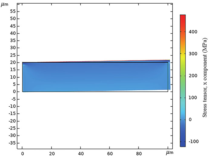
After growing the SiO2 dielectric film on the surface of the epitaxial layer, due to the different thermal expansion coefficients between materials, the lattice mismatch between the epitaxial layers will increase during the thermal annealing process at high temperatures, which will cause stress. However, the release of stress may lead to the rupture of the medium layer and engender a large number of defects in the material. For this reason, the strain of the GaAs epitaxial layer and SiO2 dielectric layer at 870 °C is simulated first.
The related material parameters during calculation and simulation are shown in Table 1. GaAs substrate is used in this research, the thickness of which is 450 μm and the total thickness of the epitaxial layer is 4.5 μm. Both the upper and lower waveguide layers contain a large number of Ga and As components, based on which the deformation state of the epitaxial layer is calculated by the deformation state of the GaAs substrate; that is, assuming the 4.5 μm epitaxial layer is an entirety and the substrate thickness is 20 μm. By employing this approach, we can avoid the calculation error caused by the large relative tolerance[15]. Then, the epitaxial layer is covered with 200 nm SiO2. The simulation results are shown in Fig. 1.
Table Infomation Is Not Enable
Figure 1.(Color online) The simulated deformation of GaAs layer and SiO2 layer at 870 °C.
It can be seen from Fig. 1 that the surface layer of GaAs is subjected to compressive stress, which can be alleviated by the outward of Ga atoms (as shown in Fig. 2).
Under the enormous tensile stress exerted by GaAs, the structure of SiO2 may be destroyed and become disordered, which further promotes the outward diffusion of Ga atoms. Although As atoms also diffuse into SiO2 during the annealing process, the diffusion rate of As atoms in SiO2 is very small compared to Ga atoms. Annealing methods also have a certain impact on the outward diffusion of Ga atoms. At the same annealing temperature, when using the rapid thermal process with a high heating rate, the external expansion rate of Ga atoms is higher than that of ordinary slow annealing in the furnace. This explains the effect of stress on the external expansion rate of Ga atoms; that is, during rapid annealing, greater stress will be generated at the interface between SiO2 and GaAs. Some theoretical studies[16] also show that compressive stress will lead to more Ga vacancies in GaAs layers, which is more conducive to quantum well intermixing.
Component interdiffusion calculation and blue shift simulation
According to the mutual diffusion of In and Ga atoms in the well and barrier regions of InGaAsP quantum well semiconductor lasers, the theoretical model of QWI can be established. Considering the one-dimensional diffusion of In atoms along the epitaxial growth direction, according to the Fick's second law, the relationship between the component concentration and time is:
Here, D is the diffusion coefficient of component atoms, and t is the diffusion time.
At the same time, the initial condition of In atomic component distribution can be expressed as:
Then, combined with the initial conditions, the component concentration distribution after In diffusion can be deduced:
The diffusion length is:
In Eq. (6), is half of the width of the quantum well, and represent the atomic component concentration in the well and barrier region respectively, erfc is the error function.
Fig. 3 simulates the distribution of In components in the InGaAsP/GaAsP single quantum well structure when the diffusion lengths Ld are 0, 1, 2 and 5 nm, respectively. When diffusion does not occur, the initial concentration of In component content in the well barrier is 0.15 and 0, respectively. At this time, the distribution of In atoms in the well and barrier regions presents an obvious step distribution. When the diffusion length is small, such as 1 nm, the concentration of In component in the well region is 0.1480, which is still large in general and is significantly different from the barrier region. Therefore, the quantum well and barrier regions can still maintain the heterojunction morphology. When the diffusion length is 2 nm, the concentration of In component in the well region is 0.1176, which declined to a certain extent, and the concentration difference of In component on both sides of the well and barrier regions decreases. With the further increase of the diffusion length, when Ld = 5 nm, the concentration of In component in the well area is 0.0569, and the concentration of In component at the interface between the well and the barrier regions gradually tends to be consistent. The obvious step distribution in the well and barrier regions has not been observed, and the heterojunction state is difficult to maintain, which also indicates that the QWI degree is sufficient. After the diffusion of In and Ga atoms is completed, the In component in the quantum well decreases, while the Ga component increases. Based on gradual abatement of In component concentration, the variations of gain spectrums of the InGaAsP/GaAsP laser were stimulated when the In component concentrations are 0.1500, 0.1480, 0.1176, and 0.0569, respectively (see Fig. 4).
Figure 3.(Color online) Variation of In composition versus the diffusion length.
It can be seen from Fig. 4 that with the decrease of In component concentration, the gain spectrum peaks gradually shift from the initial 915 to 845 nm; that is, the wavelength becomes shorter, and the blue shift occurs. For this reason, to obtain the appropriate NAW blue shift degree, maintain the good crystal quality of the active region, and ensure the optical characteristics of the lattice structure[17]. It is necessary to control the mixing degree of the components, including selecting the appropriate annealing temperature and annealing time, as well as the thickness and properties of the grown SiO2 dielectric film.
Experimental method and process
The experimental samples that are used in this project were grown on n-GaAs substrate by AIX200/4 system low-voltage MOCVD equipment, and the growth temperature was 600 °C. Primary epitaxial structure and complete epitaxial wafer structure are marked as sample 1 and sample 2, respectively, as shown in Figs. 5(a) and 5(b). Among them, sample 1 includes 500 nm GaAs buffer layer, 1950 nm AlGaAs lower confinement layer, 980 nm AlGaAs lower waveguide layer, 20 nm GaAsP upper and lower barrier layer and 6.8 nm InGaAsP quantum well combined active region, 420 nm AlGaAs upper waveguide layer, and 9 nm GaAs ohmic contact layer. The material and composition ratio of sample 2 and sample 1 are the same from the buffer layer to the upper waveguide layer. The difference is that sample 2 includes a 1100 nm AlGaAs upper confinement layer and a 150 nm GaAs ohmic contact layer.
After the growth of the samples is completed, the PL spectrums of the samples were tested. Then, PECVD is used to grow a layer of SiO2 dielectric film on the surface of the epitaxial wafers of sample 1 and sample 2, with thicknesses of 50−300 nm. The growth conditions are shown in Table 2.
Table Infomation Is Not Enable
When the dielectric film is grown, we separated the samples into 6 × 6 mm2 small standard square pieces, following which these pieces including sample 1 and sample 2 were put into an RTP-500 rapid thermal annealing furnace for experiments under the same condition. According to the relevant experimental results of our research group[18, 19], the annealing temperature range is set to 830−870 °C. The effects of annealing temperature, annealing time, and dielectric layer thickness on quantum well intermixing were investigated. After annealing, the SiO2 dielectric layer and the GaAs ohmic contact layer on the sample surface were removed. Then, the epitaxial wafer surface was cleaned with acetone and isopropanol solution. Finally, a photoluminescence spectrometer was used to test the sample. The test temperature is 300 K and the laser source adopts a 532 nm wavelength.
Experimental results and analysis
Effect of annealing temperature on PL spectrum of samples
Sample 1 and sample 2 were annealed and the annealing time was set at 180 s, with annealing temperatures of 830, 850, 870, and 890 °C, respectively. The PL spectrums are shown in Figs. 6(a) and 6(b).
Figure 6.(Color online) The PL spectrums at different annealing temperatures. (a) Sample 1; (b) Sample 2.
It can be observed that with the increase of annealing temperature, the wavelength blue shift of sample 1 and sample 2 both gradually increase, which may be the result of the mutual diffusion of In and Ga atoms. Under the same annealing condition, the wavelength blue shift of sample 1 is larger than that of sample 2. At 850, 870 and 890 °C, the blue shift difference between the two is 10, 7.3 and 10.1 nm, respectively. When the temperature is high, the PL peak intensity will decrease when compared with the original sample. At 870 °C, the PL peak intensities of sample 1 and sample 2 are 60% and 76% of the original sample, respectively. The full width at half maximum (FWHM) at each temperature of the two samples is within range of 3 nm. Therefore, to avoid the impact of high temperature on the lattice quality, the primary epitaxial wafers can be annealed at a lower temperature to achieve a suitable NAW of 30 nm blue shift. Then, we can choose 830 °C as the annealing temperature. At this temperature, the blue shift is close to 30 nm, which meets the requirement of the blue shift.
For InGaAsP/GaAsP compound semiconductor materials, QWI mainly depends on the diffusion of point defects and the interdiffusion coefficient of point defects is greatly affected by temperature, which can be expressed as:
Here, and are constants related to lattice structure and crystal material, and are the diffusion rates of group Ⅲ vacancies and interstitial atoms respectively. and represent the normalized thermal equilibrium concentrations of group Ⅲ vacancies and interstitial atoms respectively, and can be expressed by the following formulas:
Here, and represent the energy to form a vacancy and an interstitial atom respectively, which also show that the vacancies and atoms have an exponential relationship with temperature. Therefore, high temperature annealing is a necessary condition for QWI. Substitute Eq. (9) and Eq. (10) into Eq. (8) to obtain the relationship between the interdiffusion coefficient and temperature:
From Eq. (11), the interdiffusion coefficient of group Ⅲ atoms also presents an exponential growth relationship with temperature. However, a temperature that is too high will damage the lattice quality of the material. At 890 °C, the PL peak strength of sample 1 and sample 2 are only 57% and 66% of the original sample, separately. Therefore, according to the experimental results, to reduce the damage of high temperature annealing to the lattice quality of the material, we can consider growing the primary epitaxial wafer first, and we reduce the annealing temperature to obtain appropriate NAW conditions. Because the primary epitaxial wafer is thin and the heating mode is tungsten lamp irradiation. From this it can be inferred that in the primary epitaxial wafer, the heat transfer between the quantum well and the quantum barrier is faster, and the point defects are easy to diffuse into the well barrier region quickly to induce QWI, and so the overall intermixing degree is greater than that of the complete epitaxial wafer.
Effect of annealing time on the PL spectrum of the samples
We fix the annealing temperature at 830 °C and change the annealing time to 60, 180, and 300 s, respectively. The PL spectrums are shown in Figs. 7(a) and 7(b). When the annealing time is increased, the blue shift of sample 1 is larger and at 60, 180, and 300 s, the blue shift of sample 1 is 2, 11.1, and 7.3 nm more than that of sample 2, respectively. According to the previous analysis, the length of point defects interdiffusion is positively correlated with time, and the increase of diffusion length will cause a change in the composition of the quantum well and barrier materials, thus changing the band gap width. Because of the short distance between the surface layer and the well region of sample 1, it is easier to diffuse defect points to the well barrier region at the same time to cause QWI. However, long-term thermal annealing will also lead to the degradation of the quality of lattice materials[20], which is not conducive to the subsequent process steps and affects the performance of the device. Therefore, under the condition of obtaining a suitable NAW, sample 1 can be rapidly annealed to reduce the annealing time. In addition, based on relevant research[21], it is also proposed that in the process of vacancy diffusion, the component concentration of Al in the waveguide layer of sample 1 is smaller than that in the confinement layer of sample 2; in combination with the Fick's first law, in the occupation of Ga vacancies, Ga interstitial atoms in the lower layer are more likely to occupy vacancies than Al, which is shown that during annealing, sample 1 produces more Al and Ga vacancies in the lower layer; and the overall point defects concentration is large. With the increase of annealing time, the atomic interdiffusion coefficient of sample 1 is large, and the degree of hybridization in the well and barrier regions is high, and so the blue shift is larger. This hypothesis also provides some references for the epitaxial design by adjusting the composition properly without affecting the quality of the epitaxial wafers.
Figure 7.(Color online) Influence of annealing time on quantum well intermixing. (a) Sample 1; (b) Sample 2.
Effect of thickness of SiO2 on the PL spectrum of the samples
PECVD was used to grow SiO2 with different thicknesses on the surface of the epitaxial wafers to explore the influence of the thickness of SiO2 on the quantum well intermixing of the primary epitaxial wafer. Based on the previous two sections, the annealing temperature was set to 850 °C and the annealing time was 180 s. Meanwhile, the grown thicknesses of SiO2 were 100−500 nm with a gradient of 100 nm. A rapid annealing treatment was then carried out and the PL spectrums were tested on the sample. The results are shown in Fig. 8.
Figure 8.Effect of different SiO2 thicknesses on the PL spectrum peaks.
Fig. 8 reveals that with the increase of thickness, the blue shifts of the PL spectrums do not show a gradual increasing trend. At 200 nm, the blue shift is the largest and the amount of blue shift is 48 nm. The FWHM and the peak of intensity of the PL spectrum at each thickness do not differ from the original sample. According to the IFVD principle, the SiO2 dielectric film is porous and Ga atoms are easily dissolved into SiO2. From this it can be inferred that with the increase of SiO2 thickness, the capacity and quantity of dissolved Ga atoms should increase. When there are more vacancies left on the surface of the epitaxial wafer, the effect of QWI should be more obvious[22]. However, the experimental results do not clearly show the inference. It is speculated that in the rapid thermal annealing, due to the heating method, the radiation degree of different thicknesses of SiO2 to tungsten lamp is different. With different thicknesses, the reflectivity of irradiated light will be distinct and the maximum difference can reach 20%. Then, the heat transfer from the tungsten lamp to the epitaxial wafer will be unequal. The worse the heat absorption is, the worse the effect of QWI will be. Just as when the thickness of the SiO2 layer is 300 nm, the degree of blue shift is low, and so it can be supposed that the heat transfer to the wafer is poor at this time. In the IFVD process, the heat transfer and temperature have an important impact on the experimental results, based on which the thickness of SiO2 dielectric film can be selected as 200 nm. Under this condition, an appropriate degree of NAW blue shift can be obtained.
Conclusion
In this paper, the impurity-free vacancy induced QWI on primary epitaxial wafers and complete epitaxial wafers is carried out. By comparing the experimental results, the blue shift of primary epitaxial wafers is larger than that of complete epitaxial wafers under the same annealing condition and the photoluminescence intensity of primary epitaxial wafers remains above 76% of the original sample wafers. Hence, in the mixing process, the primary epitaxial wafers can be mixed to increase the bandgap at the cavity surface, and then the complete structure can be grown by combining the secondary epitaxial technology, following which the device can be prepared according to the subsequent process flow. The annealing temperature and time can be cut to reduce the damage of the annealing process to the lattice quality. In addition, in the process of analyzing the diffusion of point defects, according to the difficulty of Ga and Al interstitial atoms occupying the vacancies, the selection of the thicknesses and the component concentrations of the waveguide layer and the confinement layer in the epitaxial design can be compromised, which has a certain reference for the epitaxial growth.
Tianjiang He, Suping Liu, Wei Li, Li Zhong, Xiaoyu Ma, Cong Xiong, Nan Lin, Zhennuo Wang. Study of quantum well mixing induced by impurity-free vacancy in the primary epitaxial wafers of a 915 nm semiconductor laser[J]. Journal of Semiconductors, 2023, 44(10): 102302