• Photonics Research
  • Vol. 12, Issue 6, 1150 (2024)
Chang-Yin Ji1,2,†, Wenze Lan3,4,†, Peng Fu3,4, Gang Wang1..., Changzhi Gu3,4, Yeliang Wang2, Jiafang Li1,7, Yugui Yao1,8 and Baoli Liu3,5,6,*|Show fewer author(s)
Author Affiliations
  • 1Key Laboratory of Advanced Optoelectronic Quantum Architecture and Measurement (MOE), Beijing Key Laboratory of Nanophotonics & Ultrafine Optoelectronic Systems, and School of Physics, Beijing Institute of Technology, Beijing 100081, China
  • 2School of Integrated Circuits and Electronics, MIIT Key Laboratory for Low-Dimensional Quantum Structure and Devices, Beijing Institute of Technology, Beijing 100081, China
  • 3Beijing National Laboratory for Condensed Matter Physics, Institute of Physics, Chinese Academy of Sciences, Beijing 100190, China
  • 4School of Physical Sciences, CAS Key Laboratory of Vacuum Physics, University of Chinese Academy of Sciences, Beijing 100190, China
  • 5CAS Center for Excellence in Topological Quantum Computation, CAS Key Laboratory of Vacuum Physics, University of Chinese Academy of Sciences, Beijing 100190, China
  • 6Songshan Lake Materials Laboratory, Dongguan 523808, China
  • 7e-mail: jiafangli@bit.edu.cn
  • 8e-mail: ygyao@bit.edu.cn
  • show less
    DOI: 10.1364/PRJ.500575 Cite this Article Set citation alerts
    Chang-Yin Ji, Wenze Lan, Peng Fu, Gang Wang, Changzhi Gu, Yeliang Wang, Jiafang Li, Yugui Yao, Baoli Liu, "Probing phase transition of band topology via radiation topology," Photonics Res. 12, 1150 (2024) Copy Citation Text show less
    Probing phase transition of band topology via radiation topology for optical analogs of the QSHEs. The graphene-like SiNx PhCSs are shown in the inset of (a). R is the distance from the center of the triangular air hole to the center of the unit cell. (a), (d) Calculated transverse electric (TE)-like band structure with R=148 nm in (a) and R=175.5 nm in (d). (b), (c) and (e), (f) Calculated far-field polarization vectors (white lines) around the center of the Brillouin zone for the four photonic bands in (a) and (d), respectively. (g) Illustration of topological phase transition of band topology with R. The insets in (g) are the field distributions of the odd modes and even modes at Γ point for the z component of the magnetic field. (h) Evolution of topological charge q with R. The units of k and kx (ky) are 2π/P and π/P (π/P), respectively. The ranges of kx and ky are from −0.1 to 0.1. The change of q after the band inversion is three for the four bands, while the change of the topological invariant (spin Chern number) of the TE1/2 (TE3/4) band is ±1 (∓1).
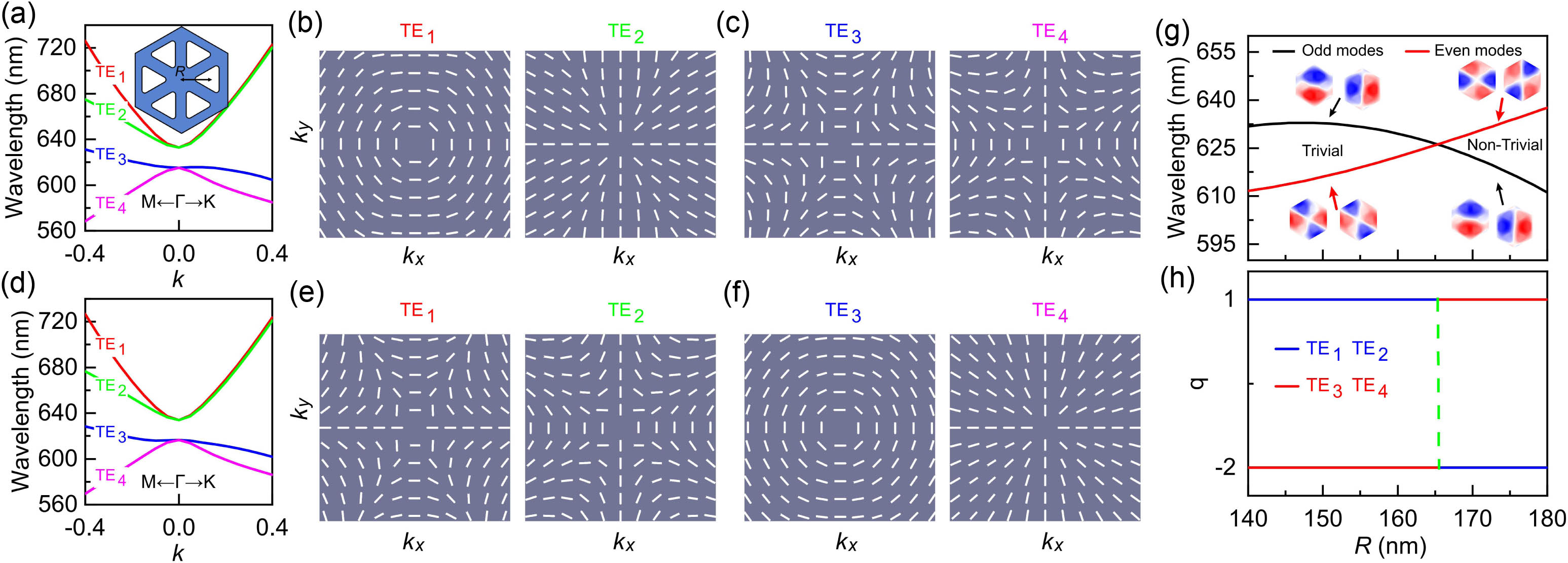
    Fig. 1. Probing phase transition of band topology via radiation topology for optical analogs of the QSHEs. The graphene-like SiNx PhCSs are shown in the inset of (a). R is the distance from the center of the triangular air hole to the center of the unit cell. (a), (d) Calculated transverse electric (TE)-like band structure with R=148  nm in (a) and R=175.5  nm in (d). (b), (c) and (e), (f) Calculated far-field polarization vectors (white lines) around the center of the Brillouin zone for the four photonic bands in (a) and (d), respectively. (g) Illustration of topological phase transition of band topology with R. The insets in (g) are the field distributions of the odd modes and even modes at Γ point for the z component of the magnetic field. (h) Evolution of topological charge q with R. The units of k and kx (ky) are 2π/P and π/P (π/P), respectively. The ranges of kx and ky are from 0.1 to 0.1. The change of q after the band inversion is three for the four bands, while the change of the topological invariant (spin Chern number) of the TE1/2 (TE3/4) band is ±1 (1).
    Probing phase transition of band topology via radiation topology for optical analogs of the SSH model. The designed one-dimensional photonic crystal is shown in the inset of (a) and Fig. 6 in Appendix A. P is the lattice period. w is the width of the SiO2 rectangular rod. The background medium is air. (a), (c) Band structures for η=0.3 in (a) and η=0.45 in (c). (b), (d) Far-field polarizations for the band structures in (a) and (c), respectively. (e) Evolution of Zak phase with η. (f) Evolution of topological charge q with η. The units of k, kx, and ky are all π/P. The ranges of kx and ky are from −0.1 to 0.1. The black dotted line in (e), (f) is the η corresponding to the bandgap closure at Γ point.
    Fig. 2. Probing phase transition of band topology via radiation topology for optical analogs of the SSH model. The designed one-dimensional photonic crystal is shown in the inset of (a) and Fig. 6 in Appendix A. P is the lattice period. w is the width of the SiO2 rectangular rod. The background medium is air. (a), (c) Band structures for η=0.3 in (a) and η=0.45 in (c). (b), (d) Far-field polarizations for the band structures in (a) and (c), respectively. (e) Evolution of Zak phase with η. (f) Evolution of topological charge q with η. The units of k, kx, and ky are all π/P. The ranges of kx and ky are from 0.1 to 0.1. The black dotted line in (e), (f) is the η corresponding to the bandgap closure at Γ point.
    SEM image and band dispersions of the band topologically trivial lattice R=148 nm in (a) and non-trivial lattice R=175.5 nm in (d). Polarization-resolved summed isofrequency contours and the corresponding Stokes phase maps of band topologically trivial lattice in (b), (c) and non-trivial lattice in (e), (f). The filtered center wavelengths in (b), (e) and (c), (f) are 640 nm and 620 nm, respectively. The 10 nm filter bandwidth in (b), (c) and (e), (f) is marked in Figs. 8(a) and 8(b) (Appendix A). The scale bar of SEM images is 500 nm. White arrows in the isofrequency contours denote the direction of the linear polarizer. The units of k and kx (ky) are 2π/P. The ranges of kx and ky are from −0.4 to 0.4 for isofrequency contours, and from −0.08 to 0.08 for Stokes phase maps. The number in the Stokes phase map is the topological charge of radiation topology.
    Fig. 3. SEM image and band dispersions of the band topologically trivial lattice R=148  nm in (a) and non-trivial lattice R=175.5  nm in (d). Polarization-resolved summed isofrequency contours and the corresponding Stokes phase maps of band topologically trivial lattice in (b), (c) and non-trivial lattice in (e), (f). The filtered center wavelengths in (b), (e) and (c), (f) are 640 nm and 620 nm, respectively. The 10 nm filter bandwidth in (b), (c) and (e), (f) is marked in Figs. 8(a) and 8(b) (Appendix A). The scale bar of SEM images is 500 nm. White arrows in the isofrequency contours denote the direction of the linear polarizer. The units of k and kx (ky) are 2π/P. The ranges of kx and ky are from 0.4 to 0.4 for isofrequency contours, and from 0.08 to 0.08 for Stokes phase maps. The number in the Stokes phase map is the topological charge of radiation topology.
    (a), (b) Schematic of a graphene-like SiNx PhCS with a hexagonal lattice of etched triangular air holes in Fig. 1. The PhCS is immersed in the air background. The thickness and lattice period of the PhCS are t=100 nm and P=496 nm, respectively. All triangular air holes have a side length of l=150 nm and a fillet of 25 nm. R is the distance from the center of the triangular air hole to the center of the unit cell. (c) Brillouin zone of the PhCS in (a).
    Fig. 4. (a), (b) Schematic of a graphene-like SiNx PhCS with a hexagonal lattice of etched triangular air holes in Fig. 1. The PhCS is immersed in the air background. The thickness and lattice period of the PhCS are t=100  nm and P=496  nm, respectively. All triangular air holes have a side length of l=150  nm and a fillet of 25 nm. R is the distance from the center of the triangular air hole to the center of the unit cell. (c) Brillouin zone of the PhCS in (a).
    Stokes phase maps for the transverse electric (TE)-like photonic bands in Fig. 1. (a), (b) Stokes phase maps for the band topologically trivial lattice R=148 nm in Fig. 1(a). (c), (d) Stokes phase maps for the band topologically non-trivial lattice R=175.5 nm in Fig. 1(d). The units of kx and ky are π/P. The number in the Stokes phase map is the topological charge of radiation topology. The band inversion mechanism can serve as an important route to explore the dynamics of topological polarization singularity and manipulate the state of polarization in the far field.
    Fig. 5. Stokes phase maps for the transverse electric (TE)-like photonic bands in Fig. 1. (a), (b) Stokes phase maps for the band topologically trivial lattice R=148  nm in Fig. 1(a). (c), (d) Stokes phase maps for the band topologically non-trivial lattice R=175.5  nm in Fig. 1(d). The units of kx and ky are π/P. The number in the Stokes phase map is the topological charge of radiation topology. The band inversion mechanism can serve as an important route to explore the dynamics of topological polarization singularity and manipulate the state of polarization in the far field.
    Designed one-dimensional photonic crystal is used to realize the well-known Su-Schrieffer-Heeger (SSH) model. P is the lattice period. h is the thickness of the SiO2 rectangular rod. h=530 nm. w is the width of the SiO2 rectangular rod. The background medium is air.
    Fig. 6. Designed one-dimensional photonic crystal is used to realize the well-known Su-Schrieffer-Heeger (SSH) model. P is the lattice period. h is the thickness of the SiO2 rectangular rod. h=530  nm. w is the width of the SiO2 rectangular rod. The background medium is air.
    P is equal to 600 nm for the results in (a)–(d). (a), (b) Band structures for η=0.3 in (a) and η=0.45 in (b). The structural parameters in (a) and (b) are the same as Figs. 2(a) and 2(c) in the main text, respectively. The insets in (a), (b), (e) are the field distributions of the y component of the electric field in the upper half space. (c) Illustration of band inversion process between odd and even modes at Γ point with increasing η. (d) Photonic eigenmodes of the supercell with sample size 15×15 [15 lattices for the structure in (a) and 15 lattices for the structure in (b)]. (e) Band structure for w=270 nm and P=550 nm. (f) Mode distributions for the edge state with sample size 15×15 [15 lattices for the structure in (a) and 15 lattices for the structure in (e)]. We have looked at the mode distribution corresponding to each eigenvalue and find no topological state on the domain wall [see (d)]. When the photonic structures on both sides of the domain wall share a common bandgap, we can clearly see the topological state on the domain wall; see (a), (e), (f). In fact we usually judge the topological phase transition of band topology experimentally by measuring whether there are topological states on the domain wall of the sample. However, this approach is very difficult to probe band topological transitions when the topologically inequivalent materials on both sides of the domain wall do not have a common bandgap. This is due to the fact that in this case there may be no topological states on the domain wall. However, the radiative topology scheme presented here directly measures the evolution of the properties of the bulk Bloch states along with the parameters without measuring the responses of the domain wall of the sample. Therefore, our method can provide another powerful tool to probe band topological transitions and may facilitate researchers to experimentally discover and realize new optical topological materials.
    Fig. 7. P is equal to 600 nm for the results in (a)–(d). (a), (b) Band structures for η=0.3 in (a) and η=0.45 in (b). The structural parameters in (a) and (b) are the same as Figs. 2(a) and 2(c) in the main text, respectively. The insets in (a), (b), (e) are the field distributions of the y component of the electric field in the upper half space. (c) Illustration of band inversion process between odd and even modes at Γ point with increasing η. (d) Photonic eigenmodes of the supercell with sample size 15×15 [15 lattices for the structure in (a) and 15 lattices for the structure in (b)]. (e) Band structure for w=270  nm and P=550  nm. (f) Mode distributions for the edge state with sample size 15×15 [15 lattices for the structure in (a) and 15 lattices for the structure in (e)]. We have looked at the mode distribution corresponding to each eigenvalue and find no topological state on the domain wall [see (d)]. When the photonic structures on both sides of the domain wall share a common bandgap, we can clearly see the topological state on the domain wall; see (a), (e), (f). In fact we usually judge the topological phase transition of band topology experimentally by measuring whether there are topological states on the domain wall of the sample. However, this approach is very difficult to probe band topological transitions when the topologically inequivalent materials on both sides of the domain wall do not have a common bandgap. This is due to the fact that in this case there may be no topological states on the domain wall. However, the radiative topology scheme presented here directly measures the evolution of the properties of the bulk Bloch states along with the parameters without measuring the responses of the domain wall of the sample. Therefore, our method can provide another powerful tool to probe band topological transitions and may facilitate researchers to experimentally discover and realize new optical topological materials.
    Experimentally measured band dispersions of the band topologically trivial lattice in (a) and non-trivial lattice in (b). The band dispersions of (a) and (b) are the same as Figs. 3(a) and 3(d), respectively. The 10 nm filter bandwidths in Figs. 3(b), 3(c), 3(e), and 3(f) are marked with purple (640±5 nm) and green (620±5 nm) dotted areas in (a), (b).
    Fig. 8. Experimentally measured band dispersions of the band topologically trivial lattice in (a) and non-trivial lattice in (b). The band dispersions of (a) and (b) are the same as Figs. 3(a) and 3(d), respectively. The 10 nm filter bandwidths in Figs. 3(b), 3(c), 3(e), and 3(f) are marked with purple (640±5  nm) and green (620±5  nm) dotted areas in (a), (b).
    Chang-Yin Ji, Wenze Lan, Peng Fu, Gang Wang, Changzhi Gu, Yeliang Wang, Jiafang Li, Yugui Yao, Baoli Liu, "Probing phase transition of band topology via radiation topology," Photonics Res. 12, 1150 (2024)
    Download Citation