
Rui Geng, Yuxin Gong. High performance active image sensor pixel design with circular structure oxide TFT[J]. Journal of Semiconductors, 2019, 40(2): 022402
- Journal of Semiconductors
- Vol. 40, Issue 2, 022402 (2019)
Abstract
1. Introduction
The potential of amorphous oxide semiconductors (AOS) for applications in large area transparent and/or flexible electronic devices has generated an incredible amount of research devoted to these materials[
Large scale image sensors also utilize TFT backplane technology which uses amorphous silicon material for the switch TFT and the photodiode in the single pixel[
The methods for driving image sensors can be categorized as passive or active. In the passive method, the exposure and readout of the sensors are performed sequentially. The majority of image sensors utilize the passive driving method because of the simple driving schematic; however, this method may introduce image blurring if fast moving objects are captured due to the pixels being subjected to exposure at different times from top to bottom of the sensor array. On the other hand, the active driving method exposes all the pixels simultaneously, and they are read out sequentially, which is favorable for the capture of moving objects. However, after exposure the charge is accumulated in the sensors from exposure until the sensor is read, which will lead to decreased image quality because of the leakage resulting from the off-state current of the shutter TFTs in the pixels. Given the very low off-state current, an active image sensor could easily be realized with a-IGZO TFTs[
In this paper, we propose a high-performance active image sensor pixel based on a-IGZO TFTs with a circular structure. The circular a-IGZO TFTs fabricated normally exhibit good performance with a mobility (μFE) of 14.3 cm2/(V·s), threshold voltage (Vth) of 3.2 V, and a subthreshold swing (SS) of 242 mV/decade. Compared to rectangular TFTs, circular TFTs exhibit good saturation electrical characteristics and much higher output resistance when configured with inner electrode as source and outer electrode as drain. This configuration results in a higher gain of voltage (close to one) when compared to rectangular TFTs. Given the very high output resistance exhibited by the circular TFTs, they can be used as the driving TFT in an active image sensor circuit. It is, therefore, a good candidate for image sensing applications such as medical diagnostic procedures.
2. Circular a-IGZO TFT
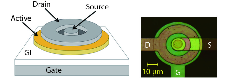
Figs. 1(a) and 1(b) show the 3-D schematic views and a microscope image of the circular a-IGZO TFTs in this work. The TFTs comprise a gate, gate insulator, active layer, outer electrode, inner electrode and passivation layer. The fabrication process is the same as the conventional back channel etched a-IGZO TFTs in rectangular shape. The 250 and 300 nm thick SiO2 layers are used as the gate insulator and passivation layer deposited by plasma-enhanced chemical vapor deposition (PECVD) at 300 °C. The 60 and 120 nm thick molybdenum (Mo) layers are used as gate and source/drain electrodes deposited by sputter. A 20 nm thick a-IGZO layer is used as active by sputter deposition at 200 °C, with a target of polycrystalline IGZO (In2O3 : Ga2O3 : ZnO = 1 : 1 : 1 mol%) and Ar : O2 gas ratio of 4 : 8. The chemical composition of the active layer deposited is determined to be In : Ga : Zn = 3 : 2 : 1 in atomic ratio. After the whole process, a 2 h thermal annealing must be carried out at 250 °C in vacuum to relieve the stress and achieve stable and reproducible performance.
![]()
Figure 1.(Color online) (a) The schematic 3-D views and (b) optical image of the circular a-IGZO TFTs.
The typical measurement results of transfer (IDS–VGS) and output (IDS–VDS) curves of circular a-IGZO TFTs with inner electrode as source and outer electrode as drain are shown in Figs. 2(a) and 2(b). The radiuses of the outer and inner electrode are 15 and 4 μm, respectively. The TFT performances in the linear regime (VDS < VGS – Vth) are very similar to the typical rectangular a-IGZO TFT in terms of the turn-on voltage, mobility from the transfer characteristic and the current level from the output characteristic; in the saturation regime (VDS > VGS – Vth), the output curve of the circular TFTs becomes flat, which means very high output resistance while the output currents of the rectangular TFT still increase with increasing VDS, indicating a low output resistance (inset is the typical output characteristics of rectangular TFT as a comparison). The devices normally exhibited a good performance with a μFE of 14.3 cm2/(V·s), Vth of 3.2 V, SS of 242 mV/decade, and ON/OFF current ratio > 10 8 for both structures. The channel length (L) of this circular TFT is determined by L = R2 – R1, where R2 and R1 are the geometrical parameters, the radiuses of the outer and inner electrodes, respectively. By considering a radial electric field, the channel width (W) of this structure should be calculated as a function of R1 and R2, it was reported as W/L = 2π/ln (R2/R1)[
![]()
Figure 2.(Color online) The typical measurement results of (a) transfer (
3. Active image sensor pixel design
The schematic of the active image sensor design is shown in Fig. 3(a), while Fig. 3(b) shows the timing diagram of this active image sensor. The single pixel of this active image sensor consists of three TFTs and one photodiode. The shutter TFT is used to control the exposure time and the switch TFT is used to read out the data when the current row is selected. The driving TFT receives the signal from the photodiode through the gate terminal and generates the output signal through the source terminal in a common-drain amplifier configuration to achieve enough drivability and less distortion. The output nodes of the entire column are biased with a single mirror current source to stabilize the output, while the whole current source of each column is mirrored to a single reference current by a single TFT in diode connection. The operation of this active image sensor consists of two steps as shown in Fig. 3(b). The shutter signal goes high and all shutter TFTs turn on, the photodiodes are exposed and the signals are stored at the gate of the driving TFT through the shutter TFT. After the exposure, the shutter TFTs are turned off and the switch TFTs are turned on by row selected for output. This common-source amplifier should have higher gain to achieve the target value of the error in gray scale.
![]()
Figure 3.The (a) schematic and (b) timing diagram of the proposed active image sensor.
4. Results and discussions
The active image sensor pixel performance was measured by swiping a voltage source instead of exposing the photodiodes for simplicity, while maintaining the shutter and switch TFTs in the on state with a consistent bias current. The equivalent circuit for this measurement is shown in Fig. 4(a).
Fig. 4(b) shows good linearity of output and gain by utilizing the circular structure for the driving TFT while maintaining a rectangular structure for the shutter and switch TFTs. It is observed that the offset voltage (Vin – Vout) exists under active load bias because the operation needs an external voltage to overcome the Vth of the driving TFT. This offset voltage can be calibrated by external or pixel circuit compensation techniques[
![]()
Figure 4.(Color online) (a) Equivalent circuit, (b) output and gain of the proposed active image sensor pixel with circular a-IGZO TFT.
5. Conclusion
We proposed a high-performance active image sensor pixel based on a-IGZO TFTs with a circular structure. The fabricated devices typically exhibited good performance with a mobility (μFE) of 14.3 cm2/(V·s), threshold voltage (Vth) of 3.2 V, and a subthreshold swing of 242 mV/decade. The circular TFTs, configured with the inner electrode as source and outer electrode as drain, exhibited good saturation electrical characteristics and much higher output resistance compared to rectangular TFTs, resulting in a higher voltage gain (close to one). Given the very high output resistance exhibited by the circular TFTs, they can be used as driving TFTs in active image sensor circuits. They are, therefore, good candidates for image sensing applications such as medical diagnostic procedures.
References
[1] T Kamiya, K Nomura, H Hosono. Present status of amorphous IGZO thin-film transistors. Sci Technol Adv Mater, 11, 044305(2015).
[2] G K Dayananda, C S Rai, A Jayarama et al. Simulation model for electron irradiated IGZO thin film transistors. J Semicond, 39, 022002(2018).
[3] J S Heo, J H Kim, J K Kim et al. Photochemically activated flexible metal–oxide transistors and circuits using low impurity aqueous system. IEEE Electron Device Lett, 36, 162(2015).
[4] L Petti, A Frutiger, N Münzenrieder et al. Flexible quasi-vertical In–Ga–Zn–O thin-film transistor with 300-nm channel length. IEEE Electron Device Lett, 36, 475(2015).
[5] G Cantarella, N Münzenrieder, L Petti et al. Flexible In–Ga–Zn–O thin-film transistors on elastomeric substrate bent to 2.3% strain. IEEE Electron Device Lett, 36, 781(2015).
[6] L T Wang, H Ou, J Chen et al. A numerical study of an amorphous silicon dual-gate photo thin-film transistor for low-dose X-ray imaging. J Display Technol, 11, 646(2015).
[7] G H Gelinck, A Kumar, D Moet et al. X-ray detector-on-plastic with high sensitivity using low cost, solution-processed organic photodiodes. IEEE Trans Electron Devices, 63, 197(2016).
[8] M Ghittorelli, F Torricelli, Z M Kovács-Vajna. Physical modeling of amorphous InGaZnO thin-film transistors: the role of degenerate conduction. IEEE Trans Electron Devices, 63, 2417(2016).
[9] Y Shao, X Xiao, X He et al. Low-voltage a-InGaZnO thin-film transistors with anodized thin HfO2 gate dielectric. IEEE Electron Device Lett, 36, 573(2015).
[10] D A Kleinman, A L Schawlow. Corbino disk. J Appl Phys, 31, 2176(1960).
[11] Y H Byun, W D Boer, M Yang et al. An amorphous silicon TFT with annular-shaped channel and reduced gate–source capacitance. IEEE Trans Electron Devices, 43, 839(1996).
[12] D Munteanu, S Cristoloveanu, H Hovel. Circular pseudo-metal oxide semiconductor field effect transistor in silicon-on-insulator analytical model, simulation, and measurements. Electrochem Solid-State Lett, 2, 242(1999).
[13] M D Ker, C K Deng, J L Huang. On-panel output buffer with offset compensation technique for data driver in LTPS technology. J Display Technol, 2, 153(2006).
[14] C L Lin, F H Chen, C C Hung et al. New a-IGZO pixel circuit composed of three transistors and one capacitor for use in high-speed-scan AMOLED displays. J Display Technol, 11, 1031(2015).
[15] M H Cheng, C Zhao, C L Huang et al. Amorphous InSnZnO thin-film transistor voltage-mode active pixel sensor circuits for indirect X-ray imagers. IEEE Trans Electron Devices, 63, 4802(2016).

Set citation alerts for the article
Please enter your email address
© Copyright 2018-2021 | Chinese Laser Press. All Rights Reserved 沪ICP备15018463号-20