1State Key Laboratory of Advanced Optical Communication Systems and Networks, School of Electronics Engineering and Computer Science, Peking University, Beijing 100871, China
2Peking University Shenzhen Research Institute, Shenzhen 518057, China
3Nano-optoelectronics Frontier Center of Ministry of Education, Peking University, Beijing 100871, China
Fenghe Yang, Pengfei Sun, Ruixuan Chen, Zhiping Zhou, "A controllable coupling structure for silicon microring resonators based on adiabatic elimination," Chin. Opt. Lett. 18, 013601 (2020)
Copy Citation Text
Optical microring resonators are extensively employed in a wide range of physical studies and applications due to the resonance enhancement property. Incorporating coupling control of a microring resonator is necessary in many scenarios, but modifications are essentially added to the resonator and impair the capability of optical enhancement. Here, we propose a flexible coupling structure based on adiabatic elimination that allows low-loss active coupling control without any modifications to the resonators. The self-coupling coefficient can be monotonically or non-monotonically controllable by the proposed coupler, potentially at a high speed. The characteristic of the coupler when implemented in silicon microring resonators is investigated in detail using substantiated analytical theory and experiments. This work provides a general method in coupling control while ensuring the resonance enhancement property, making active coupling control in a resonator-waveguide system feasible.
Optical microring resonators (MRRs) are versatile photonic building blocks in a wide range of applications from optical communication[1] and nonlinear optics[2] to quantum optics[3] and sensing[4]. The optical resonance enhances light–matter interaction, which gives rise to nonlinear and quantum phenomena, and can respond even to tiny variations in the environment. Nevertheless, the desired sensitivity also poses a challenge of coupling light into them. Fabrication error[5], temperature fluctuation[6], and device aging[7] are the main causes that make coupling conditions differ from expected. Several methods have been proposed to address this issue and can be roughly categorized into passive trimming and active tuning. The former is represented by post-fabrication trimming[8]. It can reliably produce the desired coupling condition by trimming the material refractive index on each optical resonator, but offers no control against the changing environment. Active tuning usually involves electro-optical[1,9] or thermo-optical[10] effects.
However, when the slow-responsive thermo-optical effect is inadequate and electro-optical doping configurations are required, additional losses are introduced inside the microrings and severely degrade the resonance enhancement, e.g., a Mach–Zehnder interferometer (MZI) can be embedded in the MRR to control the coupling condition for modulation[1,11], but part of the microring needs to be doped and act as a phase shifter in the MZI. As a result, the resulting quality factor (-factor) may well be reduced by 1–2 orders of magnitude due to phase shifter induced optical loss[12] and undermines the very attractiveness of resonators. Recently, a special three-waveguide coupling system (TCS) configuration insensitive to phase shifter loss was reported in the straight waveguide coupling system[13]. In analogy to the two-photon Raman adiabatic elimination (AE) process in atomic physics, the central waveguide is intentionally index-mismatched and thus effectively holds little optical power but merely acts as a conduit of energy transfer between the other two waveguides. However, due to the implementation of the Kerr effect, which is a relatively small effect when compared with the plasma dispersion effect, the coupling control capability of the previously reported configuration is limited[13–15].
In this work, we propose a flexible coupler based on the AE process so that the lossy electro-optical tuning mechanism, such as the doping structure utilizing the plasma dispersion effect, can be employed for coupling control without any modifications to the MRRs. We derive the coupling coefficients in the coupling region under the AE condition and further establish the transmittance function of the AE-based coupler, thus forming a consolidated analytical theory, which shows good agreement with numerical and experimental results. Based on the proposed analytical theory, the tuning capabilities for coupling coefficients and the resulting coupling loss (CL) are provided, showing that the tuning in the dark-state waveguide (DWG) still affects the coupling coefficients, but its loss is barely “felt” by the resonance system.
Sign up for Chinese Optics Letters TOC. Get the latest issue of Chinese Optics Letters delivered right to you!Sign up now
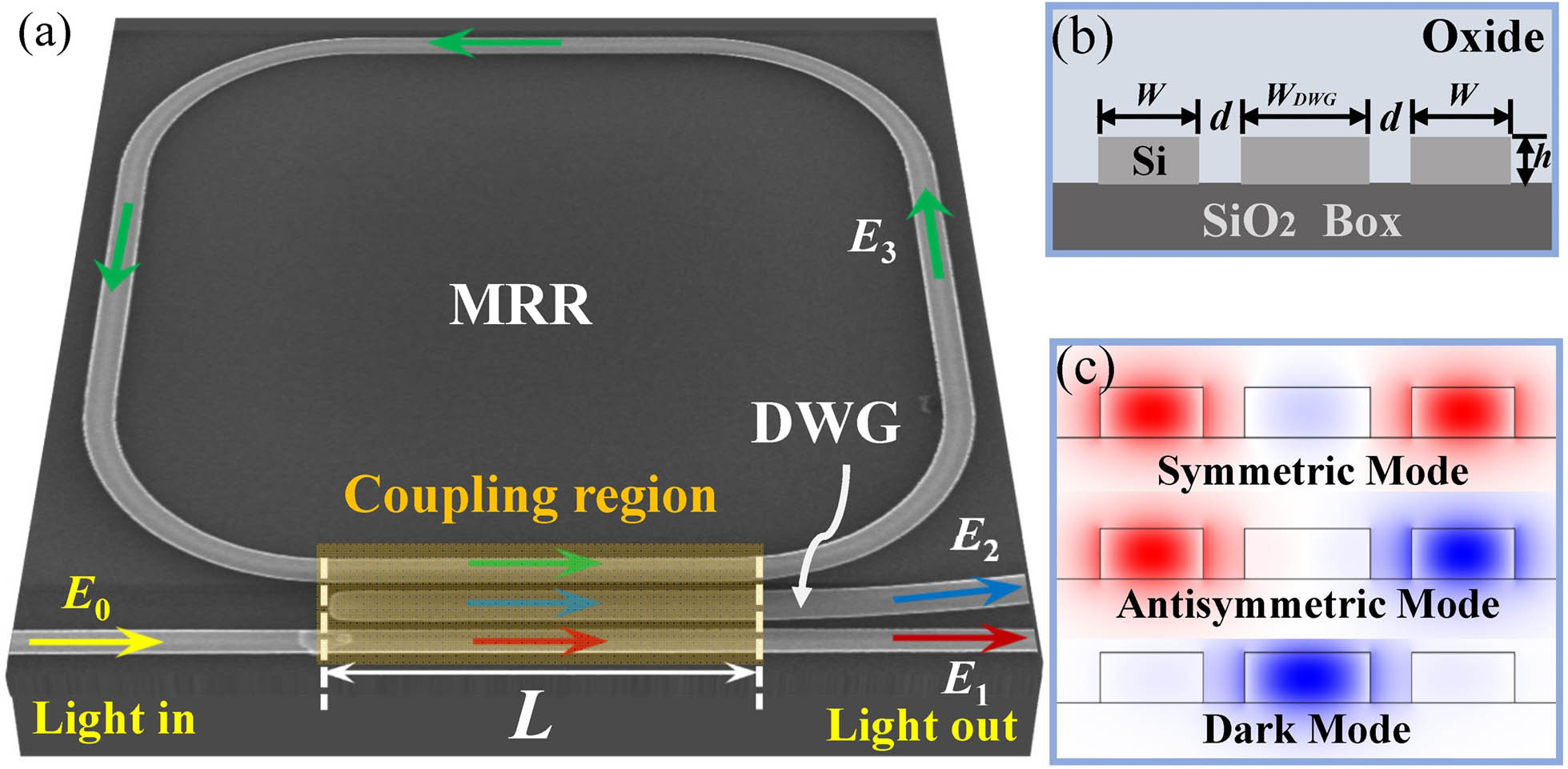
The proposed AE-based coupler [Fig. 1(a)] contains a DWG between the optical resonator and input waveguide. The cross-section view of the coupling region is shown in Fig. 1(b). In this work, the proof-of-concept verification is performed on the silicon-on-insulator platform and only one eigen state of polarization is considered in the fabricated single-mode waveguides. The top silicon layer and buried oxide layer thicknesses are 220 nm and 2 μm, respectively. The gap is fixed to in light of the fabrication capability. The waveguide widths are chosen to have large index mismatch (AE condition[13]). Two-dimensional finite element method (2D-FEM) numerical simulation shows an effective index difference () of 0.23 of the fundamental transverse electric () mode at the 1550 nm wavelength for and . The AE condition is verified by inspecting the supermodes of the TCS, i.e., symmetric mode, antisymmetric mode, and dark mode in Fig. 1(c).
Figure 1.(a) Scanning electron microscope (SEM) image of the AE-based coupler for the resonator-waveguide coupling system. (b) The cross section of the coupling region and (c) eigen modes in it.
We separate the AE-based coupler from the resonator-waveguide coupling system and analyze it as an AE-based TCS to derive the coupling coefficients. In each waveguide, the scalar field can be expressed as , where and are the optical envelope and mode propagation constant, respectively, with , and is the time-dependent phase. We adopt the shorthand notation , where and are the optical angular frequency and speed of light, respectively. Therefore, , , and can be rewritten as , , and , respectively. In this case, the coupled mode equation[16] along the whole coupling region, between and , can be transformed as the following (see Supplementary Materials):
The coupling coefficients between the adjacent waveguides are defined as , which can be taken as real and positive without loss of generality; is the optical propagation loss in DWG, needing detailed analysis in the following. The other two waveguides are passive and thus considered lossless. The solutions are as follows with the boundary conditions , , and (see Supplementary Materials):
From the expression of , we can infer that when increases, i.e., the significant index mismatch between the adjacent waveguides, tends to , so is expected to be zero. In this situation, the dark mode only resides in the DWG, while the two remaining supermodes almost have no distribution in the DWG. The DWG is expected to act as a mediator in the energy transfer between the other two waveguides. The effective self- and cross-coupling coefficients in the coupling region, and , can be expressed as and , respectively (see Supplementary Materials). However, it is worth considering that because of finite , a little power still resides in the DWG, and the optical propagation loss in the DWG also causes extra energy loss, making and less than one, and a small amount of CL is introduced (see Supplementary Materials). Therefore, the transmittance function in the proposed AE-based coupler should rigorously include the power in the DWG and the optical propagation loss, shown in Eq. (3), combined with resonance theory[17] (see Supplementary Materials). The electric field transmittances and are given by , , and , where and denote the optical resonator roundtrip loss and the phase shift per circulation, respectively:
The proposed structure was fabricated based on complementary metal–oxide–semiconductor (CMOS)-compatible silicon photonics fabrication process at the Institute of Microelectronics of the Chinese Academy of Sciences (IMECAS). The AE-based coupler, which will be embedded into the resonator-waveguide coupling system by using different lengths, was tested first. The optical intensity evolution in the three waveguides was recorded experimentally in a set of devices with different lengths near the three-dimensional finite element method (3D-FEM) simulated coupling length (μ), shown in Fig. 2, together with analytical results of Eq. (2) and 3D-FEM simulation. A tunable continuous wave laser together with a polarization controller is utilized to provide light input with desired polarization. Light is then grating-coupled into the device, and the output light is grating-coupled out to an optical spectrum analyzer for recording optical power. From Fig. 2, we observed that the power of the DWG is suppressed and oscillates very rapidly in comparison to the slow varying amplitude in the outer waveguides 1 and 3, behaving as the AE procedure as expected. These experimental results verify the proposed AE-based coupler initially and confirm the absence of optical power inside the DWG.
Figure 2.Intensity evolution along the AE-based coupler. Here, and, in the analytical model, FEM simulation, and experiments .
Three MRRs with AE-based coupler lengths μ, 20 μm, and 40 μm are characterized theoretically and experimentally, as shown in Fig. 3. The circumference of the MRRs is fixed to 300 μm to obtain an appropriate free spectral range of around 2.5 nm. Because the resonator linewidth is much smaller than coupler bandwidth, the coupling strength of the coupler can be considered as constant near the resonant wavelength.
Figure 3.Spectral responses of the fabricated resonator-waveguide coupling systems with embedded AE-based coupler: (a) under-coupled state, (b) critically coupled state, and (c) over-coupled state. The insets are SEM images. Here, in the analytical model, FEM simulation, and experiments .
In the resonance system, the condition is known as critical coupling, while the over-coupling and under-coupling conditions are defined as and , respectively[17]. As the coupling length increases, the resonator goes from the under-coupled to critically coupled and finally to the over-coupled state. The MRR roundtrip loss in analytical theory of Eq. (3) is extracted from a linear-regression-based approach[18,19]. At resonant wavelengths, the normalized intensity of the DWG is about 0.2, otherwise it remains almost zero. As for under-coupled and over-coupled states in Figs. 3(a) and 3(c), respectively, the peak normalized intensity of the DWG is around 0.1, lower than in the critical coupling state because of low cavity resonance depth. The rapid oscillation makes the DWG unable to pile up a stable electrical field, except that the incidence is around the peak wavelength when cavity resonance enhancement happens. Under all three coupling conditions, the analytical model, simulation, and experiment results match well in terms of the spectrum shape, width, and the peak normalized intensity of the DWG, consolidating the AE-based resonator-waveguide coupling theory.
A typical method for high-speed tuning of the effective index in the DWG is to leverage the silicon plasma dispersion effect and form a positive–negative (PN) junction, as widely used in silicon modulators[1,9,20]. Figure 4(a) shows two typical PN junctions, including lateral and vertical structures[1,20], in the proposed coupler to implement the active coupling control for the silicon MRR, where is a function of the reverse bias. Considering the CMOS compatibility, we choose the lateral PN junction structure for a discussion on tunability and loss. Figure 4(b) shows the results of the effective coupling coefficients in response to the DWG effective index, according to the impurity and carrier distributions in an exemplary phase modulator described in Ref. [20]. From Eq. (2), and are dependent on . Therefore, the coupling coefficients of the coupler, which are directly related to the amount of coupled light ( and ), can be tuned dynamically for coupling control. It is worth noting that short lengths, such as μ, 20 μm, and 40 μm in the previous part, are not suitable to achieve an effective coupling coefficients adjustment over a limited range of refractive index changes ( to 0.001, typically[1,9,20]) because of insufficient phase change accumulation. Considering that varies periodically with the length of DWG in the coupler, shown in Fig. 2, returns to the value of around 20 μm for the first time at around 200 μm and obtains a critical coupling state with sufficient phase accumulation according to Eq. (2). Taking coupling modulators as an example, they require the self-coupling coefficient to change from one to ( for passive optical resonators) for no coupling and critical coupling. The tuning range in Fig. 4(b) is sufficient for these applications, and by tuning the effective index of the DWG, coupling control can be implemented by the proposed coupler without any modifications to the MRRs.
Figure 4.(a) Lateral PN junction and vertical PN junction applied in the proposed AE-based coupler. (b) The effective self-coupling coefficient depending on the changes of the real part of . (c) Extra coupling loss depending on the changes of the loss coefficient . The length is μ for all lines. The MZI is assumed to be balanced.
Further analysis results indicate can be monotonously increased or reduced, even non-monotonously controlled at the proper length , shown in Fig. 4(b) (see Supplementary Materials). The needed length of the PN junction in the DWG (around 200 μm) is much shorter than one quarter of the wavelength of the electrical driving signal when implementing high-speed active control; therefore, the active area of the DWG is equivalent to a lumped load. Since the electro-optic bandwidth is limited only by the resistor–capacitor (RC) constant and is independent of the cavity photon lifetime[1], the proposed AE-based coupler can potentially provide high-speed electro-optic modulation.
Finally, we analyze the CL characteristics of the coupler when active coupling control is performed. The optical propagation loss and the residual power inside the DWG are essentially in the form of CL to the resonance system, i.e., . In the coupling region, the CL can be obtained by calculating the loss of energy propagating in the outer two waveguides, as Eq. (4) shows (see Supplementary Materials). When the AE condition is perfectly satisfied, , thus , obviously shown by the purple line in Fig. 4(c). In this case, there is no power at all inside the DWG, and the optical propagation loss has no effect on CL. When the AE condition is approached as closely as possible but is inevitably finite, there will be a small but non-negligible amount of energy residue in the DWG. In this case, the optical propagation loss and the residual power inside the DWG show a very limited effect on the CL, as shown by the green lines in Fig. 4(c). The maximum CL is only around 1 dB at a huge propagation loss for ():
We further narrow the DWG of the AE-based coupler to 400 nm without any propagation constant difference, making the structure completely deviate from the AE condition. The analytical model and simulated results show that the CL rapidly increases and approaches 3 dB when increases. It can be predicted that when implementing a wider DWG to obtain larger , the introduced CL due to the presence of DWG can be further reduced. The CL of utilizing an MZI embedded in MRRs is also analyzed, as in coupling modulators. Similar to the nature of single waveguide propagation loss, it rises linearly in the decibel (dB) scale. In all of the above analysis, the analytical model of Eq. (4) and simulation are in reasonable agreement. From Figs. 4(b) and 4(c), the proposed AE-based coupler can achieve coupling control with a suppressed CL by tuning the effective index of the DWG so that the lossy electro-optical tuning mechanism, such as doping structure, can be applied flexibly, and no modifications are needed inside the MRRs.
In conclusion, we demonstrated a novel coupling structure based on AE processing. A consolidated analytical theory, including AE-based coupled mode theory in the coupling region and the transmittance function of the AE-based coupler, is established and experimentally verified. We systematically analyze the tuning ability of the demonstrated AE-based coupler and explore the influence of the DWG on the introduced CL. By tuning the effective index of the DWG, the AE-based coupler can be employed for monotonical and non-monotonical coupling control without any modifications to the MRRs, while maintaining resonance enhancement properties.