Disposable devices designed for single and/or multiple reliable measurements over a short duration have attracted considerable interest recently. However, these devices often use non-recyclable and non-biodegradable materials and wasteful fabrication methods. Herein, we present ZnO nanowires (NWs) based degradable high-performance UV photodetectors (PDs) on flexible chitosan substrate. Systematic investigations reveal the presented device exhibits excellent photo response, including high responsivity (55 A/W), superior specific detectivity (4x10¹⁴ jones), and the highest gain (8.5x10¹⁰) among the reported state of the art biodegradable PDs. Further, the presented PDs display excellent mechanical flexibility under wide range of bending conditions and thermal stability in the measured temperature range (5–50 °C). The biodegradability studies performed on the device, in both deionized (DI) water (pH≈6) and PBS solution (pH=7.4), show fast degradability in DI water (20 mins) as compared to PBS (48 h). These results show the potential the presented approach holds for green and cost-effective fabrication of wearable, and disposable sensing systems with reduced adverse environmental impact.
Introduction
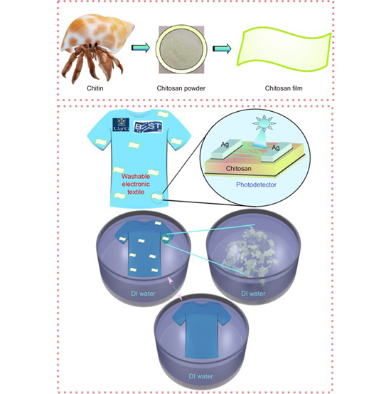
Sensor laden wearable, conformable and smart systems hold great promise for wide range of applications which includes health monitoring1-3, rehabilitation4, artificial skin in robotics2,4-9, environment monitoring10, and Internet of Things (IoT)11,12 etc. Often these applications, require cost-effective disposable sensors for short-term or single-shot measurements13,14. For example, single use sensors in wearables could help overcome the challenges related to washability. Likewise, in health monitoring applications such disposable sensors could help address the hygiene requirements. Motivated by these advantages, significant research efforts have been made for the development of disposable sensors and transient electronics, including flexible and/or stretchable form factors1,3,15. However, disposability does not necessarily mean biodegradability and this is where many of the reported devices fall short of expectations and do not fully address the growing issue of electronic waste16. Thus, more innovations are needed in both green materials and manufacturing techniques to develop eco-friendly disposable sensors. Herein, we present high performance disposable photodetectors (PDs) for smart textiles having no adverse impact after the end of use. Disposable and flexible ultra-violet (UV) PDs are critical for harmful UV detection17-19, wearable dosimetry20-22, secure communication23, health and environmental monitoring24, and many other applications. Particularly, high performance, conformal, and disposable PDs, as wearable patch, could be used to monitor exposure to UV radiations, which could lead to nonmelanoma and melanoma skin cancers25. To this end, highly flexible and green (biodegradable) materials-based devices are needed over nonplanar surfaces such as clothes or skin for wearable dosimetry. Devices with such features also come with added benefit of alleviating the growing problem of electronic waste. Such wearable and disposable patches can be used for real-time monitoring of UV radiation under diverse environmental conditions such as mountaineering activities.
Owing to large surface to volume ratio, excellent mechanical strength, efficient charge transport and ability to form heterostructures, the one-dimensional (1D) nanowires (NWs), and 2D materials such as graphene have gained immense interest as active UV sensing materials for low-cost flexible UV PDs. Among these the ZnO nanostructures are most studied and used in different device architectures/configurations19,26-28, due to distinct advantages they offer over the other 1D materials, including (i) cost-effective synthesis methods, (ii) multi-functional properties (e.g. semiconducting, energy harvesting etc.), (iii) environmental friendliness, and (iv) biocompatibility and biodegradability29-32. However, most of the reported ZnO NW based UV PDs, so far, have been realized on non-biodegradable and/or non-recyclable substrates. The high-performance ZnO NWs based PDs demonstrated here have been developed on fully biodegradable chitosan substrates (Fig. 1). The sensing and substrate materials are carefully selected so that the device could harmlessly degrade in water during washing of sensors-integrated clothes. Among wide variety of natural, abundant, and eco-friendly biomaterials (e.g., silk, collagen, cellulose, keratin, egg albumin, chitosan etc.33-35), chitosan has been selected as a substrate due to its chemical stability, good optical transparency, greater mechanical flexibility, and excellent biodegradability14,36,37. Further, the fabrication steps used for presented devices are eco-friendly, scalable, and resource efficient. These include synthesis of chitosan based green substrates, spray coating of ZnO NWs, and screen printing to realize electrodes. Systematic UV photodetection studies, performed under wide range of light intensities (0.1 μW/cm2 to 2 μW/cm2) and bias voltages, show excellent response of developed devices. These include good responsivity 55 A/W, excellent detectivity 4×10¹⁴ jones, higher gain 8.5×10¹⁰, good external quantum efficiency 104, linear dynamic range of 72 dB, and fast response (0.7 s) and recovery (0.8 s) time. Further, the PDs showed stable and robust performance under different bending (10–40 mm) and thermal range (5–50 °C) of UV sensing measurements. These systematic investigations show that the presented devices meet the unique “5S” (sensitivity, selectivity, stability, signal-to-noise ratio, and response speed)38,39 requirement for many applications. Finally, the biodegradability tests reveal that the presented device can degrade and dissolve in DI water and PBS in less than 20 min and 48 h respectively.
Figure 1.Schematic showing the concept of biodegradable and disposable UV photodetectors for smart textiles leaving no toxic residues.
The flexible and biodegradable chitosan films were prepared using the conventional spin coating process followed by drying on a hotplate at 40 °C for approximately 10 h. The as prepared films were then explored as a substrate for the fabrication of the UV PDs. Next, screen printing was utilized to print silver electrodes over two ends of the NW-network film formed by spray-coating technique40. Screen printing was employed owing to its excellent attributes such as resource-efficiency, substrate independent patterning, compatibility with large area manufacturing, and the potential for low-cost operation41,42. The details of the fabrication process are provided in the experimental section. The thin chitosan films show excellent flexibility and good optical transparency (>80% at 550 nm) which is confirmed from the transmittance plot depicted inFig. 2(a). Further, to determine the optical energy band gap (Eg) of the ZnO NWs, UV- visible spectroscopy measurements were performed.
Figure 2.UV-visible spectroscopy studies. (a) Transmittance plot of chitosan with the optical image of the prepared chitosan film, and (b) absorbance plot of the ZnO NW with the inset showing the taucs plot with the calculated band gap. (c) Low and (d) high magnification SEM images of ZnO NWs.
Figure 2(b) shows the absorption spectra of the ZnO NWs with a maximum absorption peak located at 375 nm, and the inset plot shows the taucs plot showing the calculated band gap energy. The optical band gap of the ZnO NW was calculated using the taucs equation stated as below:
where α is the molar extinction constant,
is the energy, K is a constant, the value of n is considered as 0.5 for the direct band gap materials and the slope of the plot (
)2 vs (
) gives the direct band gap of the ZnO NWs. The calculated band gap energy of the material (3.3 eV) matches well with the previously reported values of ZnO NWs43. To further examine the structural properties, XRD was performed on the ZnO NWs (
Fig. S1). The diffraction peaks at 2θ angles of 32.5°, 34.3°, 37.1°, 48.5°, 57°, 63.6°, 68.9°, and 81.2° correspond to the crystal planes of (100), (002), (101), (102), (110), (103), (112), and (104), respectively. The obtained XRD peaks confirm the highly crystalline of ZnO NWs, which matches well with the literature. The high intensity diffraction peak at 25° corresponds to the substrate. Figure 2(c–d) show the low and high magnification images of ZnO NWs. There are no impurities present. Further, the calculated average length and diameter of the NWs were ~10 μm and ~175 nm, respectively (
Fig. S2(a–b)). The spray coated ZnO NW-network is expected to have a strong adhesion strength with the chitosan44, and exhibit high porosity which helps during the adsorption and desorption of oxygen anions during UV detection.
The UV photo response of the fabricated PDs was measured under 365 nm wavelength UV light source and characterization results are shown in Fig. 3. The long duration exposure of the high intensity UV light (λ=365 nm) on skin or eyes causes severe skin allergies and carotenal damage and hence the detection of that wavelength is important. Schematic representation of the fabricated ZnO NW based printed PDs is shown inFig. 3(a).Figure 3(b) shows the absolute current-voltage (I-V) plot of the PD under both dark and UV illumination at different intensities (0.1 to 2 μW/cm2) for an applied voltage bias ranging from –5 V to +5 V. The results indicate that the device exhibits characteristics of a typical back-to-back symmetrical Schottky contacts19. This is because silver metal is expected to form Schottky contacts with the lightly doped semiconducting ZnO NWs. Further, significant enhancement in device current was observed with an increase in UV power intensity. The I-V characteristic is shown in the supporting information
Fig. S3. Next, the systematic studies related to photo response characteristics were performed under different power intensities and various bias voltages. Figure 3(c) shows the time-dependent UV response characteristics of the device under different power intensities for different bias voltages (1 V–5 V with the step of 1 V). The photo current increases from 1 nA under dark conditions to 4 μA in the presence of UV light at a power intensity of 2 μW/cm2 and applied bias voltage of 5 V. Under these conditions the device shows excellent photo response characteristics with a high IPhoto/Idark ratio of 4×10³. The device exhibits a linear increment in current for different intensities showing repeatable and stable device performance. Furthermore, it can be clearly seen that the photo current gradually increases with the bias voltage varying from 1 to 5 V.
Figure 3.ZnO NWs based printed PD and electrical characterization results. (a) Schematic of the fabricated device. (b) Absolute current vs voltage plot. (c) Light illuminated temporal response characteristics at different bias voltages (1–5 V) under different UV illumination intensities. (d) Stepwise incremental response under different light intensities from 0.1 to 1.1 μW/cm2. (e) Cyclic stability, and (f) linear dynamic response plot under different illumination intensities.
The temporal photo response characteristics of PDs were obtained by applying different power intensities from 0.1 to 1.1 μW/cm2 with a power interval of 0.1 μW/cm2 as shown in Fig. 3(d). The obtained results reveal that the current gradually increases from 1 nA to 2 μA for different power intensities, which further demonstrates the linear incremental response of the device. The cyclic repeatability of the fabricated device was tested for 10 cycles under a constant applied bias of 5 V at an illuminated light intensity of 2 μW/cm2 which exhibits a uniform and stable cyclic behavior (Fig. 3(e)). Linear dynamic range (LDR), defined as the linear dependance of the photo current on the light intensities, is one of the important parameters of the PDs which can be analyzed using theEq. (2) below28:
where
,
are the current densities under light illuminated and non-illuminated conditions. The LDR plot of ZnO NWs based PD under different UV light intensities and different voltage bias are shown in Fig. 3(f). These results show a maximum LDR value of 72 dB which is comparable with the previously reported ZnO based PDs28. Besides, the device is tested under visible and infrared (IR) light with different intensities and no response in these conditions suggests excellent selectivity to UV illumination.
The fabricated PD devices were further evaluated in terms of photoresponsivity (R), specific detectivity (D*), external quantum efficiency (EQE) and gain etc. using the response current, photon flux, and illuminated optical power. This quantitative analysis is given in Fig. 4. The R and D* are the two major important performance parameters of the PDs as they mainly determine the sensitivity of the device. R is the ratio of the response current to the incident power which is obtained as45:
Figure 4.(a) Responsivity. (b) Detectivity. (c) External quantum efficiency. (d) Response and recovery time. (e) Current on/off ratio. (f) Photoconductive gain of the photodetector at different bias voltages varying from 1 V to 5 V under different light intensities.
where
is the photo current and
is the incident light power per unit area. The calculated responsivity at an illuminated wavelength of 365 nm under different bias voltages from 1 to 5 V and multiple power intensities is depicted in Fig. 4(a). The device provides excellent R >55 A/W. Further, the PD showed response to low UV intensity of 0.1 μW/cm 2, suggesting the capability to detect lower power intensities. Such a high responsivity at low UV intensity could be attributed to the use of high-quality, high aspect ratio, and large number of NWs in the sensing channel19,46. Moreover, it is observed that higher responsivity was attained at larger bias voltage and higher applied power intensities owing to the larger generation of e-h pairs. D* is one of the vital figures of merit of the PD which is closely related with the different noise currents and R of the device and is calculated as28:
where
is the dark current density and q is the charge of the electron. As per Eq. (4), higher R and lower dark current densities are needed to achieve high detectivities. The calculated D* values under different illuminated power at multiple applied bias voltages are shown inFig. 4(b). The ZnO NW-based device exhibits high D* value of 4×10¹⁴ Jones at an applied bias voltage of 5 V, owing to the high responsivity and very lower dark currents. The obtained high R and D* values could be attributed to the presence of multiple blocking contact points by forming multiple barriers at the NW-NW interface resulting in the lower device dark currents. The high-performance PDs especially with higher R and D* are very much needed for the detection of low intensity optical power signals useful in some of the biomedical applications47. Next, the external quantum efficiency (EQE), which is the reciprocal of the noise equivalent power, was calculated as48:
where
is the wavelength of the incident light. Figure 4(c) shows the EQE of the NW-based PD at different UV intensities from 0.1 to 2 μW/cm2 operated at a bias voltage ranging from 1 to 5 V in steps of 1 V. The fabricated device exhibits a good EQE even at lower power intensities and an increasing trend with the increase in the operating voltage similar of responsivity. A maximum of 1×10⁴ EQE (%) was exhibited under the illuminated power intensity of 0.3 μW/cm2 at an applied bias voltage of 5 V.
A faster response is needed along with the stable sensor performance. The measured response time (tres) and recovery time (trec) are shown in Fig. 4(d). The device rises quickly in a short tres of 0.7 s and then decays trec quickly within 0.8 s. The tres and trec here represent the time difference between the 10% of the saturated photo response current to the 90% and vice versa. The response/recovery times are faster than most of the previous works (Table 1), but also slightly slower than some of these. The slow response could be attributed to the presence of surface defects in ZnO NWs. Passivation techniques could be explored in future to have a faster photo response from the PD device49,50. The sensitivity of the PD is the measure of the ratio between the photo response current to the dark current. The on/off ratio of the device at various illuminated UV power intensities under different bias voltage is shown inFig. 4(e). The device exhibits higher current on/off due to the stable and lower dark current values which are in the order few hundred of picoamperes. Besides, R and D*, the photoconductive gain (G) is other important parameter and is defined as the ratio of number of the charge carriers (Ne) collected at electrodes to the number of incident photons (Np) in the device active area. It can be obtained as28:
where
is the net photo response current,
is the energy of the photon,
is the active area of the device,
is the incident power. The calculated gain values are presented in Fig. 4(f), and the device exhibits a maximum gain of ≈ 8.5×10¹⁰ at an incident power of 0.3 μW/cm2 and at a lower bias voltage of 1 V. This is the highest among the reported state of the art PDs based on ZnO NWs. The higher gain of the as fabricated device is primarily owing to the longer carrier lifetime of the photogenerated carriers in the NWs as compared to the transit times during the transport between the electrodes. With such a high gain PD it is possible to detect even a small intensity optical signal. Further, a decreasing trend in the gain with bias voltage was observed, which matches well with the literature19. The high-performing PDs especially higher gain, responsivity and detectivity are useful in biomedical applications to detect very weak signals.Table 1 shows the comparison of our device with other ZnO NWs based UV PDs.
The obtained high PD performance is explained using the schematics and energy band diagram shown in Fig. 5. The UV sensing mechanism for ZnO NW based PDs is well documented in the literature. It is known that the point defects near the NW surface play a critical role in the UV sensing. The oxygen molecules present in the atmosphere get adsorbed onto these defect sites resulting in forming a depletion region owing to the capture of free electrons (O2+e–
O2–), as illustrated with a blue line in Fig. 5. The as formed depletion region creates an internal electric field in the radial direction, due to the overall band bending at the metal-semiconductor (MS) interface. When illuminated with UV light greater than the bandgap of the ZnO NWs, electron-hole (e-h) pairs are generated. The photogenerated e-h pairs get separated due to the internal electric field and transported to the electrodes (Fig. 5). The generated radial field helps in suppression of photocarrier recombination and dramatically prolonged carrier lifetimes. Meanwhile, the adsorbed oxygen anions get resorbed by combining with the generated holes and thus, increase in the concentration of free electrons in the channel. This results in the decrease of MS barrier width (effective barrier height) and an overall enhancement of drain current. However, in the present case, the observed high device performance can be correlated to the additional energy barriers (current ‘blocking’ points) present at the NW-NW junctions. For a single NW based PD device, the dark current is usually higher because of the difficulties in realizing high-quality Schottky contacts. This is due to the excess charge carriers present in the NW because of the thermal activation at room temperature. Higher dark current limits the current on/off ratio and detectivity of the PD devices. In comparison to this, in the present device, there exist large number of NW-NW junctions between the two Schottky contacts. These NW-NW junctions serve as extra potential barriers for carrier transport under dark condition and introduce additional band-edge modulation along axial direction of the sensing channel28 (Fig. 5). Consequently, the dark current of the printed PDs can be largely suppressed. The temperature dependent measurements (
Fig. S4) were performed to extract the activation energy of the device, which includes potential energy at back-to-back metal-semiconductor (MS) contacts and barrier energy which exists between various NW-NW connecting sites. The activation barrier energy of the device is extracted from the Arrhenius plot which comes to be 0.4 eV. When illuminated with the UV light, the generated excess charge carriers in the NWs lead to the lowered barrier potential energy at the NW-NW junctions. Because of these simultaneous physical phenomena, there is large reduction of the channel resistance and thus, the PD device demonstrates a high current gain.
Figure 5.Schematic representation of UV sensing under dark, explaining adsorption of oxygen from ambient air and formation of depletion layer and under illumination condition the electron-hole pair generation followed by the physical desorption and sensing mechanism explained with the help of energy band diagram for Ag/ZnO/Ag photodetector device.
Biodegradable sensors could easily collapse under different types of stress/strain including heat, mechanical bending etc. Besides, wearable sensors should demonstrate stable device response under wide temperature range as ambient temperature could vary depending on seasons/geography. Accordingly, a systematic temperature dependent photo response study of the ZnO NW based PDs devices was performed and the resulting performance is shown in Fig. 6. The photo response characteristics of the fabricated PD under illuminated light intensities of 0.1, 0.5, 1, 1.5, 2 μW/cm2 at different temperatures (15 to 45 °C with a step of 10 °C) is performed (
Fig. S5). The results indicate a good thermally stable behavior under different temperatures. As expected, the dark current increases with an increase in temperature. This is because charge carriers acquire adequately higher kinetic energy with an increase in the temperature to overcome the potential barrier and thus, thermionic emission current increases53. On the other hand, the photo current (under UV illumination) showed negligible enhancement. This could be understood as follows: Increasing the temperature leads to increased thermal vibrations, resulting in the increase in scattering events (acoustic phonon assisted and Coulombic) as well. This will lead to decrease of electron mobility and degrade the quality of charge transport and thus reduction in the device current. However, as mentioned earlier, there is also enhancement in the thermionic current with the temperature increase. Therefore, the trade-off between these two distinct phenomena defines the output current to increase or decrease under different illumination conditions. The R (Fig. 6(a)), EQE (Fig. 6(b)) and G (Fig. 6(c)) show negligible increase with the temperature change. This is because these parameters are proportional to the device on-current. As the illumination current remains almost constant with the temperature increase, there is no degradation of these performance parameters. However, the D* (Fig. 6(d)), current on/off ratio (Fig. 6(e)) and LDR (Fig. 6(f)) of the device showed slight decrease with the temperature increase. This is due to their dependence on the device dark current (under no UV illumination). D* is inversely proportional with the dark current. As discussed above, under no UV, the dark current increases due to an increase in the thermionic current component and therefore, D* decreases. Likewise, the slight degradation of the Ion/off ratio and LDR is due to the increase in the dark current of the device with increasing temperature.
Figure 6.Temperature dependent performance stability data for ZnO NW printed PDs: (a) responsivity, (b) external quantum efficiency, (c) photoconductive gain, (d) detectivity, (e) on/off ratio, and (f) linear dynamic range of the device under different UV intensities.
To understand the mechanical robustness of the fabricated device, bending studies were performed under three different bending radii: 40 mm, 20 mm, 10 mm at a constantly applied power intensity of 0.5 μW/cm2 and the results are shown in Fig. 7(a, b and c), respectively. Robust PD performance can be observed from this set of data. To further understand the effect of bending on the device performance, all the performance metrics were calculated and compared with the device under flat condition. Here, 180 mm is considered as the device under flat condition for comparison.Figure 7(d) shows the comparison plot of R (left) and D* (right) y-axis under different concave bending radius: 40 mm, 20 mm, 10 mm and flat condition. The data shown indicate that R values slightly increase with the decrease in bending radius. One possible reason for an increase in the R is the strong NW-NW interactions resulting in the reduction of contact or junction resistance at the interface19. The reduction in the junction resistance might slightly affect the conductivity of ZnO NW’s network and hence lead to a slight increase in the photo response current. The device exhibits similar trend in the D* values primarily due to the directly proportional relationship with the photo response current. A plot displaying the comparison of the G (left) and LDR (right) calculated at a constant illuminated power intensity of 0.5 μW/cm2 is shown inFig. 7(e). The obtained results show there is a slight increase in both G and LDR of the PD. This is owing to the slight increase in the photo response current.Figure 7(f) shows the current on/off ratio and EQE (%) of the fabricated ZnO NW based PD under different bending radius and flat condition. The device exhibits a meagre variation in both the on/off ratio and EQE, thus demonstrating its excellent stability and mechanical robustness under bending conditions.
Figure 7.The temporal response characteristics of PD under different bending radii. (a) 40 mm, (b) 20 mm, (c) 10 mm and comparison of different performance parameters of the photodetector (d) responsivity, detectivity (e) gain, linear dynamic range (f) on/off ratio, EQE under different bending radius (note that 180° was considered as the device under flat condition).
The biodegradability study was also performed on the as prepared ZnO NW-based PDs in both deionized (DI) water and phosphate buffered saline (PBS) solution with pH of 7.4, as shown in Fig. 8. The biodegradation studies should be performed in accordance with the existing standards for plastics degradation54. In the present work, the degradation measurements were performed in ambient environment at room temperature.Figure 8(a) to8(e) show the optical images of the device in DI water after 3 s, 1 min, 5 mins, 10 mins, and 20 mins, respectively. When the device is immersed in DI water, the chitosan substrate (due to its excellent hydrophilic nature) quickly absorbs the water in few seconds and swells, as can be seen from theFig. 8(b). Afterwards, the device gets physically disintegrated due to the easily breakable glycosidic bonds present in the polysaccharide of chitosan. Next, the several functional groups in the chitosan such as hydroxyl, amino, carbonyl, amido etc. react with DI water and degrade to produce a non-toxic oligosaccharide, which are further converted to the non-toxic glycoproteins55. From the dissolution experiments, it was observed that the device completely gets dissolved in DI water in less than 20 mins with some minor traces of silver electrodes left floating and the NWs were completely dispersed in the DI water, as shown inFig. 8(f). Although, silver is not biodegradable its excellent conductivity, biocompatibility and antibacterial property made it as an good starting material for exploration of different electronic applications and for future work it can be effectively replaced with some of the biodegradable metals such as zinc or magnesium56. A low molecular weight chitosan was chosen here for the preparation of the biodegradable substrate owing to its higher degradation rate in aqueous medium as compared to its higher molecular weight55,57. Although the silver nanoparticles are not biodegradable, silver exhibit biocompatibility, antibacterial properties and the screen-printed approach reduces the overall cost of the device fabrication as compared to the traditional physical vapor deposition methods58. Due to their excellent antibacterial and antimicrobial properties, silver nanoparticles have been explored recently for different biological applications such as wound healing, drug delivery, and smart bandages56.
Figure 8.Biodegradability test of as fabricated device showing periodic degradability at different times in DI water. (a) 3 s showing absorption of water due to hydrophilic nature of chitosan. (b) Swelling of the chitosan after 60 s. (c) Physical disintegration after 5 min. (d) 80% of the device dissolved and (e) complete dissolution with only non-toxic screen-printed silver traces after 20 min. The outcome of dissolution tests repeated in PBS (pH=7.4) (f) after 10 s, (g) 10 min, (h) 30 min and (i) after an hour showing slight physical disruption of the device.
The device degradation study was also conducted in PBS solution and the results are shown in Fig. 8(f–i) for distinct times – 10 s, 10 min, 30 min, and 60 min respectively. The PBS was chosen here because it is a balanced salt, a good biofluid and pH value can be maintained at 7.4 to match with the properties of the biofluids. The degradation rates of device in the PBS solution (pH=7.4) were lower as compared to the DI water (pH≈6) under the same condition, primarily due to the difference in the pH values. Generally, the solubility of the chitosan is higher in weak and/or diluted weak acids such as acetic acid. In fact, the dissolution rate is mainly governed by the presence of amino groups which exhibits strong basic nature and easily gets converted to a polyelectrolyte when the amino groups get protonated. As a result, chitosan dissolves quickly in aqueous acid mixtures and the solubility rate reduces for slightly basic medium i.e., for pH values > 7 59. Similar trend was seen here (Fig. 8(i)) from the experiments as the device slightly got physically disintegrated after 60 min. The device got completely dissolved after 2 days at room temperature.
It is important to highlight that the demonstrated PD devices are categorized into partially biodegradable. The substrate (chitosan) and active sensing layer (ZnO NWs), which constitute most of the device weight, are non-toxic, environment-friendly green materials34,60. However, the PD device also comprises of non-biodegradable printed silver. The toxicity and biodistribution studies for Ag nanoparticles (NPs) are being investigated with various routes61. Presently, there is lack of information in the risk assessment of the Ag in the form of NPs both for humans and the environment. The hydrometallurgical treatments on extracted silver particles could be used to recycle most of the disintegrated silver and enhance the circularity in electronics62. Further, based on the biodegradability studies, it can be argued that moisture and/or sweat could affect the PD performance and thus, the device may not be effective for wearable applications. However, such issues can be overcome by suitable packaging. For example, by applying nanocoating of materials such as perylene. Highly conformal perylene coatings can be deposited at room temperature. It has low permeability to moisture and is also biocompatible63. The conformal thin coatings at the back side of the device substrate can resist water and body sweat, protecting the photodetector function and performance during wearable applications.
Conclusion
In summary, we have reported high-performance biodegradable UV PDs developed using green materials and fabrication process. The UV PD demonstrates excellent and repeatable photo response under different bias voltages with a high responsivity (55 A/W), superior detectivity (4×10¹⁴), and higher gain (8.5×10¹⁰). The high performance of presented degradable PDs can be attributed to the presence of multiple energy barriers because of multiple NW-NW junctions, which act as extra blocking contact sites for electrons. The temperature dependent measurements showed the activation energy (0.4 eV) of the device is high enough to reduce the device dark current. The PD also showed stable and robust performance under thermal and mechanical stress. This is needed for accurate and reliable measurements in the case of wearable applications where body movements (strain) and changes in ambient temperature could lower the PD performance. Finally, biodegradability studies were performed in both DI water and PBS which showed biodegradation as fast as 20 mins. Thus, the simple, and resource efficient approach presented for the fabrication high performance disposable PDs could also reduce the adverse environment impacts of electronics fabrication and disposal.
Experimental section
Materials
The ZnO NWs were purchased from the Novarials Corporation. 2-proponal (>99% pure), chitosan (low molecular weight), and acetic acid (>99% pure) were purchased from the sigma Aldrich. The silver conductive paste was purchased from sun chemicals.
Preparation of chitosan thin films
The 4 wt.% of low molecular weight chitosan powder was mixed in 1% v/v of acetic acid in DI water and stirred for approximately 24 hours. The solution was casted in a polystyrene petri dish and kept at the room temperature for 24 hours to allow formation of moderately thin films. The dried films were used as a flexible substrate for the fabrication of the device.
Fabrication of screen-printed electrodes
Silver electrodes was printed using the Screen Printer C920 from AUREL Automation. A constant force of 25 N was applied on the 15 cm long squeeze with less than 1 mm distance between the squeeze and the screen. Afterwards, the process was repeated twice, and the samples were sintered at 60° in an oven for an hour to remove the solvent. Sheet resistance (~2 Ω/sq) was measured using Osilla four-point probe measurement setup.
Material characterization: The transparency of chitosan thin film and the absorbance of the ZnO NW were measured using shimadzu 2600 UV spectrometer for a spectral range of 200 nm – 900 nm. The X-ray Diffraction (XRD) studies were performed using the PAN analytical Xpert pro varying from 200 nm to 900 nm. Scanning electron microscopy (SEM) was carried out using the FEI nova SEM MPD diffractometer Cu Kα radiation (λ = 1.54059 Å(1 Å=0.1 nm)) over the 2θ range of 10°–60° with steps of 0.05°.
Photodetector device fabrication and characterization
The device was fabricated using spray coating ZnO NWs on the electrodes screen-printed on flexible chitosan substrate and the active area of the device is 0.03 mm2. The active sensing area is calculated according to the dimensions of the screen-printed electrode (L (150 µm) × W (200 µm)). A commercial UV LED of wavelength (λ=365 nm) was used for the photo illumination studies and the light intensity of 0.1–2.1 μW/cm2.
References
[30] Shakthivel D, Ahmad M, Alenezi MR, Dahiya R, Silva SRP. 1D Semiconducting Nanostructures for Flexible and Large-Area Electronics: Growth Mechanisms and Suitability (Cambridge University Press, Cambridge, 2019).