
Junpeng Liao, Ye Tian, Zirong Yang, Haoda Xu, Chen Tang, Yuheng Wang, Xiaowei Zhang, Zhe Kang. Inverse design of highly efficient and broadband mode splitter on SOI platform[J]. Chinese Optics Letters, 2024, 22(1): 011302
- Chinese Optics Letters
- Vol. 22, Issue 1, 011302 (2024)
Abstract
1. Introduction
In recent years, integrable mode-division multiplexing (MDM) systems have attracted increasing attention due to their great potential in further improving the transmission capacity of on-chip optical interconnection[1,2]. To assemble a complete MDM system, various key building elements have been proposed, such as mode (de)multiplexers [(De)MUXers][3,4], mode filters[5,6], mode converters[7,8], and multimode bendings[9,10]. In addition to these multimode devices, the mode splitter is a crucial component that straightforwardly separates modes of different orders into different channels. Currently, most reported mode splitters are established by implementing the mode (De)MUXers. These (De)MUXers enable mode separation by converting the high-order modes into the fundamental mode and mapping them to the specific channel via a phase-matching mechanism. However, in the case of a mode-sensitive system, mode conversion with mode orders changes would lead to instability and performance degradation of the system[11,12]. Therefore, a mode splitter without changing the mode orders is highly preferred and can effectively improve the flexibility of the MDM system.
To date, only a few studies have been reported on the mode splitters without changing mode orders, because directly splitting modes with different effective indices within the same waveguide is quite challenging. Liao et al. proposed a mode splitter based on an asymmetric directional coupler (ADC)[13]. The splitter consists of two slits and a strip waveguide that can separate the and modes with cross talk (CT) of and insertion loss (IL) of for a 100 nm bandwidth range. In Ref. [14], a dual-mode mode splitter was designed by introducing small slots in the silicon waveguide to form a symmetric directional coupler (DC), achieving CT of and low IL of for the entire C-band. Furthermore, a dual-mode splitter for separating and modes was developed using a bridged subwavelength grating-assisted (BSWG) DC and a mode filter, with CT of and IL of for a bandwidth of 84 nm[15]. However, these designs cost a large footprint of hundreds of micrometers squared, and the device structures are also complex. More recently, intelligent design methods for photonic devices have been extensively investigated, offering advantages in reducing device size and improving design efficiency[16]. However, little research has been conducted on mode splitter design using such methods. In Ref. [17], a mode splitter was designed by using the direct binary search (DBS) algorithm. The optimized device has an ultracompact size but exhibits a high IL of 3.04 dB, which is unsuitable for practical applications. Therefore, designing a high-performance mode splitter in a small footprint remains a challenge.
In this paper, we use a shape optimization method to design a high-performance mode splitter without changing the mode orders. Our design method is able to optimize multiple design objectives simultaneously and requires only four simulations per iteration, effectively improving device performance while increasing device design efficiency. Using this method, we designed and fabricated a mode splitter with a compact footprint of only , which separates and modes with an IL of and a CT of over a broad bandwidth range of 1500–1600 nm. To the best of our knowledge, this device achieves the broadest operation bandwidth for this level of performance in such a compact size. Additionally, we demonstrate the generality of the shape optimization method by designing a dual-mode (De)MUXer, with experimental results indicating an IL of below 1 dB and a CT of below within the 1500–1600 nm bandwidth range.
Sign up for Chinese Optics Letters TOC. Get the latest issue of Chinese Optics Letters delivered right to you!Sign up now
2. Design and Simulations
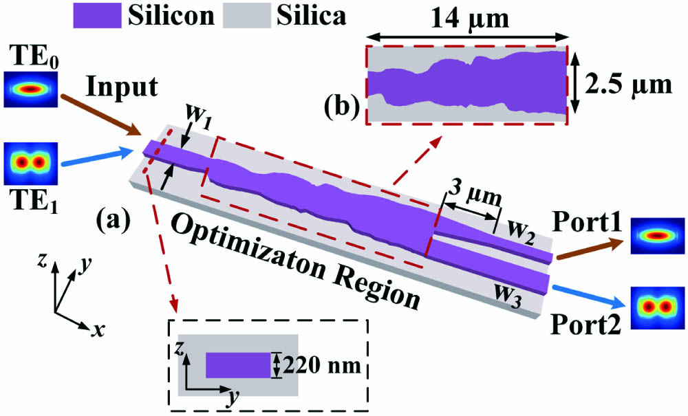
Figure 1(a) depicts the schematic diagram of the proposed mode splitter, which is designed on the silicon-on-insulator (SOI) platform with a 220-nm core silicon layer, a 2-µm buried oxide layer, and a 1-µm top oxide cladding. The width of the input waveguide is set as 1 µm to support both and modes, while the widths of Ports 1 and 2 ( and ) are set as 500 nm and 1 µm to support and modes, respectively. The optimization region is labeled with a dotted box with an area of . As shown in Fig. 1(b), the boundary curves distort when approaching the design target as the shape optimization runs. After optimization, the mode is output from Port 1, while the mode from Port 2 without changing the mode orders. Note that a tapered waveguide with a length of 3 µm is introduced between Port 1 and the optimization region. The primary objective is to mitigate backscattering effects and concurrently enhance the optical transmission of light. The width of the tapered end is set as 500 nm for compatibility with the standard single-mode access, while the width of the initial portion is set as 1 µm to ensure a separation exceeding 200 nm between the tapered waveguide and Port 2.
![]()
Figure 1.(a) Schematic diagram of the proposed mode splitter; (b) boundary shape of the mode splitter.
The flow of designing a mode splitter using the shape optimization method is shown in Fig. 2. The optimization objective is quantified by the figure of merit (FOM). and are defined as the average transmittance of the target mode for the two output ports in the designed bandwidth,
![]()
Figure 2.Design flow of the mode splitter. (a) Initial structure of the device; (b) simulation stage of device design; (c) optimization of the device shape using Python; (d) optimized structure of the device.
The shape optimization method used in this study consists of two stages. The first stage involves simulating the device using the 3D finite-difference time-domain (FDTD) method, as shown in Fig. 2(b). To improve the optimization efficiency, the adjoint method is introduced, which enables the calculation of the gradient of FOM with respect to the geometrical parameters from the solution of Maxwell’s propagation equations and requires only two runs of simulation for each iteration: one for the forward solution and one for the adjoint solution, which greatly improves the design efficiency[18]. The gradient of and with respect to the material boundary can be found using the adjoint method[19], which can be written as
The second stage involves optimizing the boundary shape of the coupler using Python, as depicted in Fig. 2(c). The gradients of and with respect to the optimized point are computed in Python, and the coordinate of the point is adjusted using the gradient descent method to maximize and , respectively, so that each FOM value converges to 1. To ensure that the optimized structure is not too sharp, numerical constraints are added to the coordinates of the adjacent points to limit their variation within . The optimized boundary shape is obtained by spline interpolation fitting of the adjusted optimized points. The simulation stage and optimization stage are run iteratively until the device meets the target performance. The final optimized mode splitter is shown in Fig. 2(d). It is worth noting that the two FOMs defined can be optimized simultaneously in each iteration to ensure simultaneous increases in and during the optimization process.
In addition to the mode splitter, we also designed a dual-mode (De)MUXer that routes either or mode to mode, demonstrating the generality of the design method. Similarly, the two optimization objectives ( and ) are defined as the average transmittance of the mode for the two output ports of the mode (De)MUXer over the design bandwidth. The evolution of the boundary shapes and FOMs for both devices during the optimization process is shown in Figs. 3(a) and 3(b), respectively. It can be observed that a balance between and is maintained throughout the optimization process and is consistently increasing simultaneously. The final geometries for both devices were obtained after around 30 iterations. In order to be able to show the shape of the designed mode splitter and mode (De)MUXer more precisely, we provide the coordinates of the points on the boundary curves of the mode splitter and mode (De)MUXer in a rectangular coordinate system, as shown in Fig. S1 (see Supplementary Material). The detailed coordinates of the 200 points that construct the upper and lower boundaries of the mode splitter/mode demultiplexer are shown in Table S1 (see Supplementary Material). The simulated electric field distributions of the mode splitter and mode (De)MUXer are shown in Figs. 3(c) and 3(d), respectively. As or is injected, it propagates to the target port with the desired mode order.
![]()
Figure 3.Boundary shape evolution and FOM evolution for (a) mode splitter and (b) mode (De)MUXer; simulated electric field distribution for (c) mode splitter and (d) mode (De)MUXer.
The transmission spectra of the mode splitter and mode (De)MUXer are presented in Figs. 4(a)–4(d), respectively. At 1550 nm, for mode injection, the IL of the mode splitter is 0.14 dB and the CT is less than . On the other hand, with mode injection, the IL is 0.15 dB and the CT is less than . In the wavelength range from 1500 to 1600 nm, the IL and CT of the mode splitter are less than 0.44 dB and , respectively, for mode injection, and less than 0.55 dB and , respectively, for mode injection. Similarly, for mode (De)MUXer, at 1550 nm, the IL and CT are 0.06 dB and , respectively, for mode injection, and 0.05 dB and , respectively, for mode injection. In the wavelength range of 1500 to 1600 nm, for mode injection, the IL and CT for mode (De)MUXer are less than 0.27 dB and , respectively, and with mode injection, IL and CT are less than 0.21 dB and , respectively.
![]()
Figure 4.Simulated transmission spectra for (a) mode splitter as TE0 input, (b) mode splitter as TE1 input, (c) mode (De)MUXer as TE0 input, and (d) mode (De)MUXer as TE1 input.
Fabrication inaccuracies are inevitable during the fabrication process. Therefore, overall tolerance analysis was performed on the deviations of the waveguide widths () for both devices, as shown in Figs. 5(a)–5(h). It can be observed that when deviates by , the IL of the mode splitter is less than 1.14 dB and the CT is less than in the wavelength range of 1500–1600 nm. When deviates by , in the wavelength range of 1500–1600 nm, the IL of the mode splitter is less than 0.84 dB and the CT is less than . Similarly, over the 100 nm wavelength range, for mode (De)MUXer, IL is below 0.55 dB and CT is below when , and IL is below 0.54 dB and CT is below when . These results demonstrate that the devices designed using the shape optimization method exhibit good fabrication tolerance.
![]()
Figure 5.Simulated transmission spectra of the mode splitter when (a) ΔW = −20 nm and TE0 input; (b) ΔW = −20 nm and TE1 input; (c) ΔW = +20 nm and TE0 input; and (d) ΔW = +20 nm and TE1 input. Simulated transmission spectra of the mode (De)MUXer when (e) ΔW = −20 nm and TE0 input; (f) ΔW = −20 nm and TE1 input; (g) ΔW = +20 nm and TE0 input; and (h) ΔW = +20 nm and TE1 input.
3. Fabrication and Measurement
The designed mode splitter and mode (De)MUXer are fabricated on a standard SOI platform with a 220 nm top silicon layer and a 2 µm buried oxide layer. The pattern of the device is defined using 193 nm-deep ultraviolet (UV) photolithography, while the Si layers are etched using inductively coupled plasma (ICP). Finally, a silica upper-cladding was deposited on the structure by the plasma-enhanced chemical vapor deposition (PECVD) process.
Figure 6(a) depicts the microscopic views of the on-chip test structures for the mode splitter. An ADC-based mode (De)MUXer, proposed in Ref. [20], was employed to generate and detect and modes. The ADC converts the light from Port into the in the bus waveguide while maintaining the light from Port . At the output, light is directly output from , while light is coupled to and output from . Figure 6(c) depicts a microscopic view of the test structure of the mode (De)MUXer. Similarly, and light is transmitted using the ADC-based MUXer. Through the fabricated mode (De)MUXer, light is directly output from , while will be demultiplexed to output from . A reference structure that connects two ADCs back to back was also fabricated for normalizing the test results, as shown in Fig. 6(b). All the ports are connected to TE-type grating couplers (GCs) with a loss of 5 dB/facet for light.
![]()
Figure 6.Microscopic view of the fabricated (a) mode splitter, (b) ADC reference, and (c) mode (De)MUXer. Zoom-in view of the fabricated (d) mode splitter and (e) mode (De)MUXer.
A tunable laser (Santec TSL-550) was used as the light source, and an optical power meter was used to measure the transmission spectra of the fabricated devices. The losses of the ADC-based mode (De)MUXer along with the GCs are deducted from the measured spectrum of the fabricated device; the measurement results are shown in Figs. 7(a)–7(d). As a comparison, the simulation results are also attached in Fig. 7 (dashed curves). The mode splitter shows an IL and CT of below 0.6 dB and , respectively, for injection over a broadband wavelength of 1500–1600 nm. On the other hand, when is injected, the IL and CT are below 0.9 dB and , respectively. For the mode demultiplexer, the ILs of both and are below 1 dB, and the CTs are below for the same bandwidth. It is worth noting that there are slight variations between the measured results and the simulated results in terms of device performance. This discrepancy can be attributed to random deviations in waveguide sidewall etch roughness and width in fabrication.
![]()
Figure 7.Normalized transmission spectra of (a) mode splitter as TE0 input, (b) mode splitter as TE1 input, (c) mode (De)MUXer as TE0 input, (d) mode (De)MUXer as TE1 input.
A comparison between our work and the previously reported mode splitters is presented in Table 1. It is obvious that the mode splitter designed in this work has better overall performance. Specifically, the fabricated device exhibits the lowest loss and largest bandwidth. Moreover, its footprint is relatively compact, with a length of only 14 µm.
| Ref./Type | Method | Length (µm) | IL (dB) | CT (dB) | BW (nm) |
|---|---|---|---|---|---|
| [ | ADC | 50 | < 1 | < −8 | 100 |
| [ | DC | 270 | < 0.1 | < −15 | 35 |
| [ | BSWG | 106 | < 1.8 | < −15 | 84 |
| [ | DBS | 5 | < 3.04 | < −16 | 95 |
| / Sim. | This work | 14 | < 0.55 | < −18 | 100 |
| / Exp. | 14 | < 0.9 | < −16 | 100 |
Table 1. Comparison of Reported Mode Splitters
4. Conclusion
In conclusion, our study presents a mode-splitter design using the shape optimization method, which is experimentally verified to be capable of separating and modes without changing their mode orders. The device has a compact footprint of and demonstrates IL below 0.9 dB and CT below over a broadband wavelength range of 1500–1600 nm. Furthermore, we demonstrate the versatility of the shape optimization design method by using the same principle to design a dual-mode (De)MUXer, which exhibits IL below 1 dB and CT below over the same bandwidth. In addition, the two devices designed are able to maintain good performance for a width variation of . Overall, the designed mode splitter and mode (De)MUXer could find application in on-chip MDM systems for broadband mode routing. We believe that the shape optimization design method used can be scalable to other photonic devices, providing an effective tool for the development of advanced integrated photonic circuits.
References
[1] C. Li, D. Liu, D. Dai. Multimode silicon photonics. Nanophotonics, 8, 227(2018).
[19] O. D. Miller. Photonic Design: From Fundamental Solar Cell Physics to Computational Inverse Design(2012).
[20] J. Wang, Y. Xuan, M. Qi et al. Ultra-broadband integrated four-channel mode-division-multiplexing based on tapered mode-evolution couplers. European Conference on Optical Communication (ECOC)(2016).

Set citation alerts for the article
Please enter your email address
© Copyright 2018-2021 | Chinese Laser Press. All Rights Reserved 沪ICP备15018463号-20