• Photonics Research
  • Vol. 6, Issue 3, 149 (2018)
Yevhenii M. Morozov1、2, Anatoliy S. Lapchuk2, Ming-Lei Fu1, Andriy A. Kryuchyn2, Hao-Ran Huang1, and Zi-Chun Le1、*
Author Affiliations
  • 1College of Science, Zhejiang University of Technology, Hangzhou 310023, China
  • 2Institute for Information Recording of NAS of Ukraine, Shpak Str. 2, Kiev 03113, Ukraine
  • show less
    DOI: 10.1364/PRJ.6.000149 Cite this Article Set citation alerts
    Yevhenii M. Morozov, Anatoliy S. Lapchuk, Ming-Lei Fu, Andriy A. Kryuchyn, Hao-Ran Huang, Zi-Chun Le. Numerical analysis of end-fire coupling of surface plasmon polaritons in a metal-insulator-metal waveguide using a simple photoplastic connector[J]. Photonics Research, 2018, 6(3): 149 Copy Citation Text show less
    Spatial geometry of the photoplastic connector: (a) view from the PH; (b) view from the excitation area.
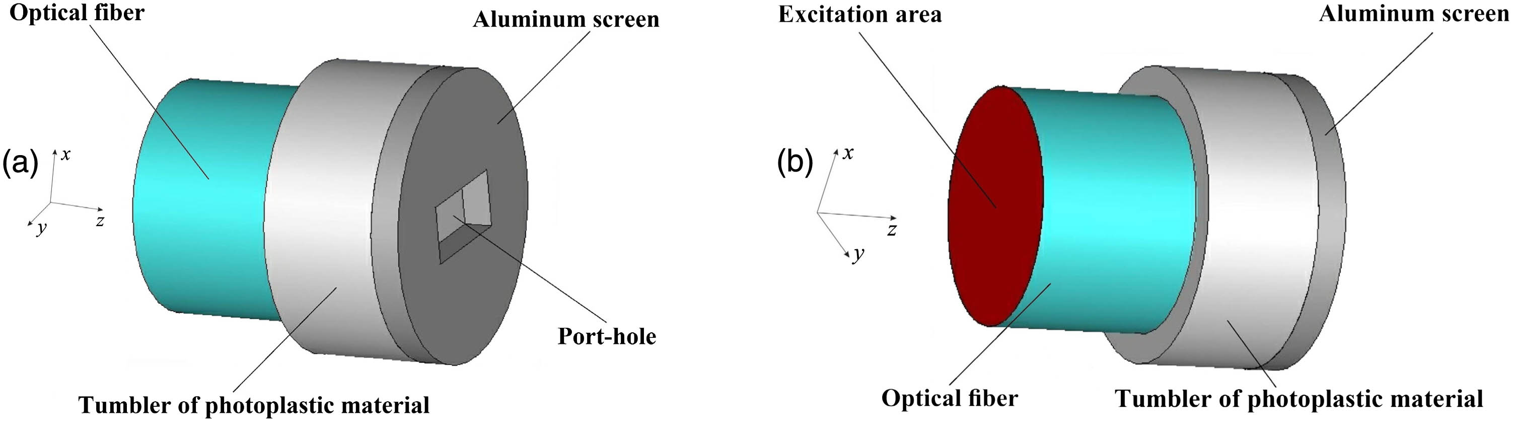
    Fig. 1. Spatial geometry of the photoplastic connector: (a) view from the PH; (b) view from the excitation area.
    Schematic representation of the connector design: (a) view from the excitation area, (b) view from the PH, and (c) longitudinal view. d1 is a diameter of the optical fiber, and thus the inner diameter of the tumbler; d2 is the external diameter of the tumbler, and thus the diameter of the Al screen; a and u are the width and height of the PH, respectively; L1 is the length of the optical fiber; L2 is the length of the tumbler; L3 is the thickness of the Al screen; L4 is the distance between the optical fiber and Al screen, that is, the thickness of the tumbler bottom; L5 is the length of the MIM waveguide; b is the thickness of the MIM waveguide dielectric layer; t is the thickness of the MIM waveguide’s metallic coatings.
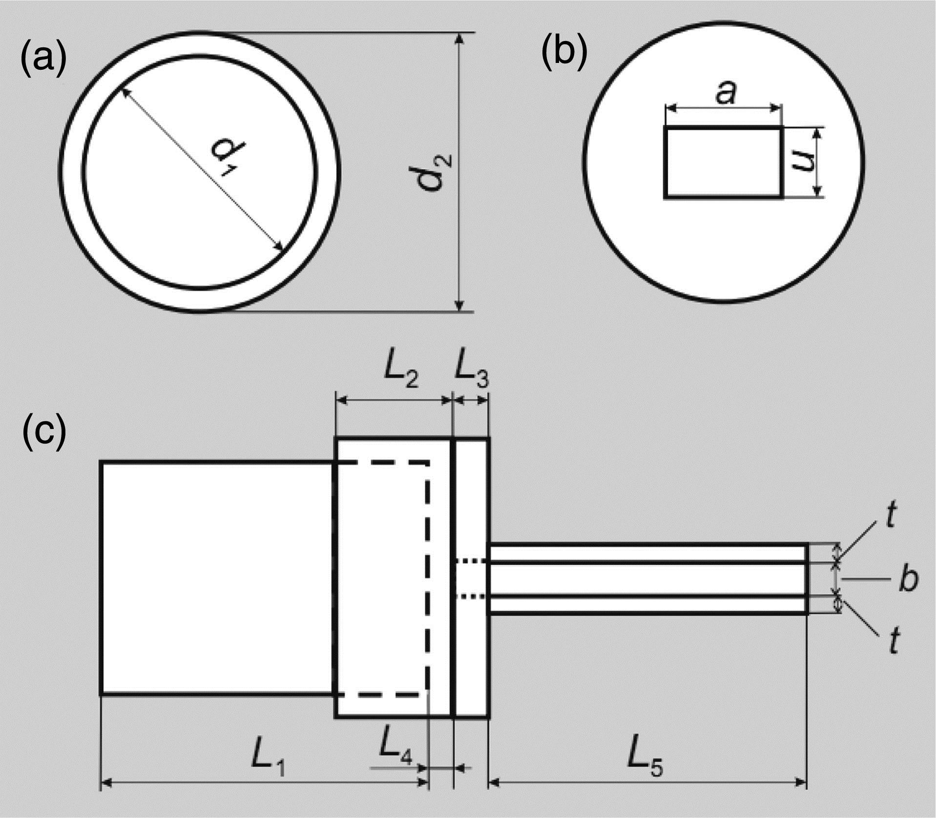
    Fig. 2. Schematic representation of the connector design: (a) view from the excitation area, (b) view from the PH, and (c) longitudinal view. d1 is a diameter of the optical fiber, and thus the inner diameter of the tumbler; d2 is the external diameter of the tumbler, and thus the diameter of the Al screen; a and u are the width and height of the PH, respectively; L1 is the length of the optical fiber; L2 is the length of the tumbler; L3 is the thickness of the Al screen; L4 is the distance between the optical fiber and Al screen, that is, the thickness of the tumbler bottom; L5 is the length of the MIM waveguide; b is the thickness of the MIM waveguide dielectric layer; t is the thickness of the MIM waveguide’s metallic coatings.
    Contour plot and profiles of the absolute value of the electric field of the fundamental propagation LP01 (HE11) mode of a circular dielectric waveguide; white dashed circle corresponds to outer edge of the optical fiber core; red dashed lines correspond to the PH dimension along the x axis; a.u., arbitrary units.
    Fig. 3. Contour plot and profiles of the absolute value of the electric field of the fundamental propagation LP01 (HE11) mode of a circular dielectric waveguide; white dashed circle corresponds to outer edge of the optical fiber core; red dashed lines correspond to the PH dimension along the x axis; a.u., arbitrary units.
    Electric field amplitude (Ex) profile of the fundamental symmetric plasmon quasi-TM00 mode; b=200 nm, t=50 nm; red dashed lines correspond to the PH dimension along the x axis; black dashed line corresponds to the |E| profile of the fundamental propagation LP01 (HE11) mode of a circular dielectric waveguide along the x axis from Fig. 3.
    Fig. 4. Electric field amplitude (Ex) profile of the fundamental symmetric plasmon quasi-TM00 mode; b=200  nm, t=50  nm; red dashed lines correspond to the PH dimension along the x axis; black dashed line corresponds to the |E| profile of the fundamental propagation LP01 (HE11) mode of a circular dielectric waveguide along the x axis from Fig. 3.
    Dependence of ceff_1 and power reflection coefficient |R1|2 on the Al screen thickness L3; d1=1000 nm, d2=1200 nm, L1=500 nm, L2=400 nm, L4=100 nm, a=500 nm, u=200 nm.
    Fig. 5. Dependence of ceff_1 and power reflection coefficient |R1|2 on the Al screen thickness L3; d1=1000  nm, d2=1200  nm, L1=500  nm, L2=400  nm, L4=100  nm, a=500  nm, u=200  nm.
    Dependence of ceff_1 and |R1|2 on the tumbler bottom thickness L4; d1=1000 nm, d2=1200 nm, L1=500 nm, L2=400 nm, L3=50 nm, a=500 nm, u=200 nm.
    Fig. 6. Dependence of ceff_1 and |R1|2 on the tumbler bottom thickness L4; d1=1000  nm, d2=1200  nm, L1=500  nm, L2=400  nm, L3=50  nm, a=500  nm, u=200  nm.
    Cross-sectional view of the electric field and energy flux in the structure: (a) x component of the electric field; (b) absolute value of the electric field; (c) z component of the Poynting vector. d1=1000 nm, d2=1200 nm, L1=500 nm, L2=400 nm, L3=50 nm, L4=100 nm, a=500 nm, u=200 nm; a.u., arbitrary units.
    Fig. 7. Cross-sectional view of the electric field and energy flux in the structure: (a) x component of the electric field; (b) absolute value of the electric field; (c) z component of the Poynting vector. d1=1000  nm, d2=1200  nm, L1=500  nm, L2=400  nm, L3=50  nm, L4=100  nm, a=500  nm, u=200  nm; a.u., arbitrary units.
    Dependence of ceff_2 on the Al screen thickness L3; d1=1000 nm, d2=1200 nm, L1=500 nm, L2=400 nm, L3=50 nm, L4=100 nm, L5=1000 nm, a=500 nm, u=200 nm, b=200 nm, t=50 nm.
    Fig. 8. Dependence of ceff_2 on the Al screen thickness L3; d1=1000  nm, d2=1200  nm, L1=500  nm, L2=400  nm, L3=50  nm, L4=100  nm, L5=1000  nm, a=500  nm, u=200  nm, b=200  nm, t=50  nm.
    Cross-sectional view of the electric field and energy flux in the structure with the MIM waveguide: (a) x component of the electric field; (b) absolute value of the electric field; (c) z component of the Poynting vector. d1=1000 nm, d2=1200 nm, L1=500 nm, L2=400 nm, L3=50 nm, L4=100 nm, L5=1000 nm, a=500 nm, u=200 nm, b=200 nm, t=50 nm; a.u., arbitrary units.
    Fig. 9. Cross-sectional view of the electric field and energy flux in the structure with the MIM waveguide: (a) x component of the electric field; (b) absolute value of the electric field; (c) z component of the Poynting vector. d1=1000  nm, d2=1200  nm, L1=500  nm, L2=400  nm, L3=50  nm, L4=100  nm, L5=1000  nm, a=500  nm, u=200  nm, b=200  nm, t=50  nm; a.u., arbitrary units.
    Yevhenii M. Morozov, Anatoliy S. Lapchuk, Ming-Lei Fu, Andriy A. Kryuchyn, Hao-Ran Huang, Zi-Chun Le. Numerical analysis of end-fire coupling of surface plasmon polaritons in a metal-insulator-metal waveguide using a simple photoplastic connector[J]. Photonics Research, 2018, 6(3): 149
    Download Citation