
Wang Xudong, Lv Xin, Cheng Gong. Terahertz vertical transition structure based on coupling cavity[J]. Infrared and Laser Engineering, 2020, 49(6): 20190566
- Infrared and Laser Engineering
- Vol. 49, Issue 6, 20190566 (2020)
Abstract
0 Introduction
Short-distance communication system operating at terahertz band has called for high transmitting power on compact structure[
In recent years, vertical transition techniques are widely developed in compact integration of active and passive circuits, such as through silicon-via (TSV) and low-temperature co-fired ceramic circuits(LTCC)[
Traditionally, vertical transition structures, are most commonly used in forms of via-hole, aperture-coupled and cavity-coupled[
Cavity-coupled transitions, however, can be regarded as an aperture in a thick common ground plane[
In this letter, the quartz media thinning and two-sided plating technologies are used to design a low-loss, 50-μm thick vertical transition structure. A mode transition technique is utilized to accurately evaluate signal transmission path. A coupling cavity is introduced to connect with the mode transition unit. Taking the advantage of good thermal conductivity of the metal wall, high power active devices can be integrated into this architecture. This vertical transition structure exhibits a potential in power combining with low insertion loss at terahertz frequency.
1 Design
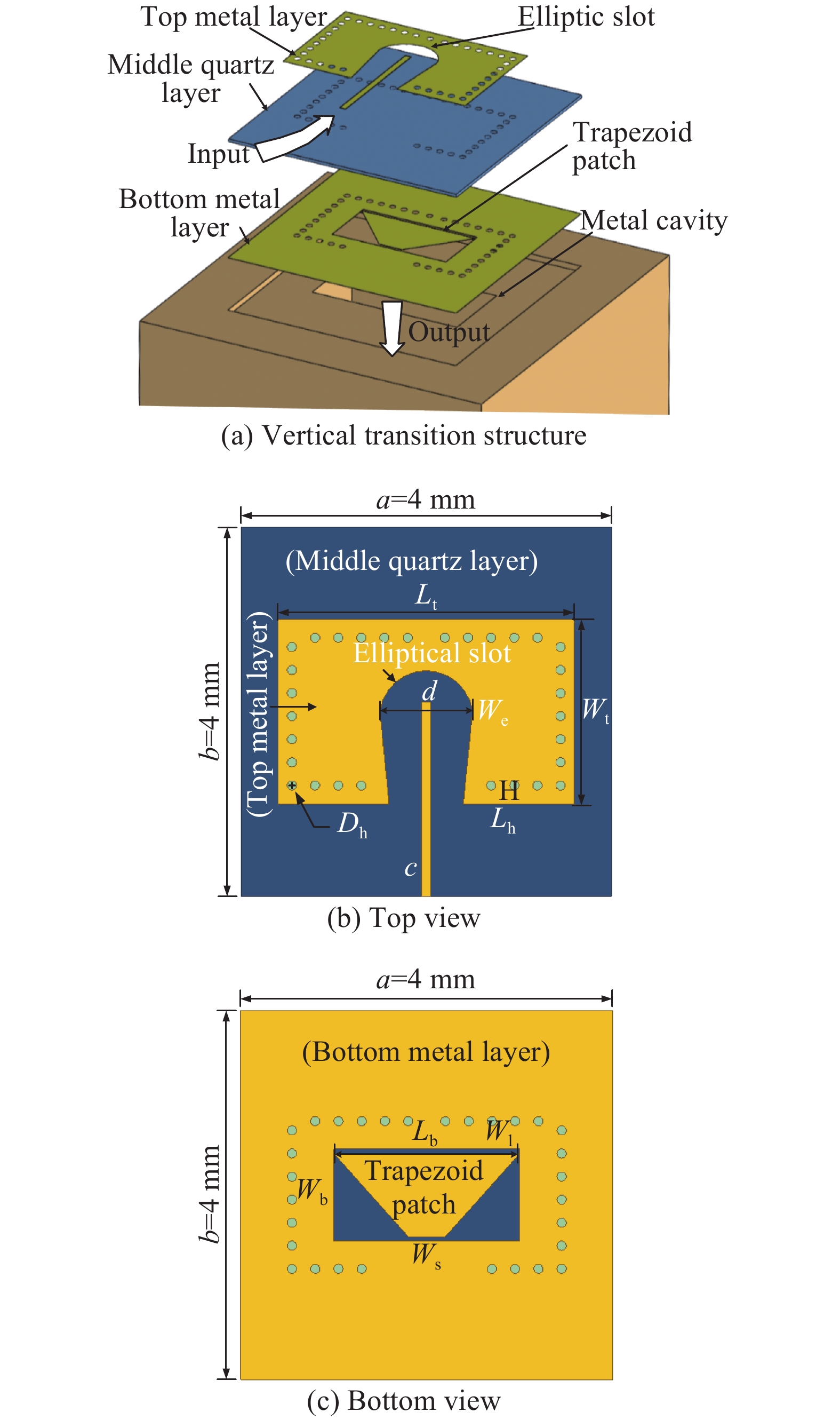
![]()
Figure 1.General vertical transition structure
On the other side of the cavity, there is a symmetrical mode-transition unit transforming signal from cavity to microstrip-line. The use of the metal cavity increases the heat dissipation capability and makes it compatible with active integrated circuit. As we can see from the
![]()
Figure 2.Designed structure of the vertical transition
Adjusting electromagnetic field distribution of the mode-transition unit is the key factor that helps transmitting guided signal from planar transition to vertical direction. Several simulations were performed to evaluate the performance of the vertical transition structure using full-wave electromagnetic simulator HFSS. As we can see from the
![]()
Figure 3.Electric-field distribution of mode-transition unit
The width We of elliptical slot is then under investigation. As the width increases, the working band width is extended. When the width Wl of trapezoid patch is changed, the transition impedance matching is affected. The larger the width Wl is, the lower the insertion loss will be. The simulation results are presented in
![]()
Figure 4.Optimization of vertical transition unit
Other than the two characters discussed above, a mass of work has been done to reach a better transition performance. For example, the length Lh between holes and the diameter Dh of the hole on quartz are designed to be 150 μm and 100 μm. Comprehensive consideration is made on basis of optimal design and engineering practice. Optimized parameters of vertical transition unit are presented in
| Parameters | Value/mm | Parameters | Value/mm | |
| 4 | 1 | |||
| 4 | 2 | |||
| 2.1 | 0.4 | |||
| 0.102 | 0.1 | |||
| 2 | 0.15 | |||
| 3.2 | 2 | |||
| 1 |
Table 1. Parameters of vertical transition unit
![]()
Figure 5.Photograph of the assembled structure and the fabricated mode-transition unit
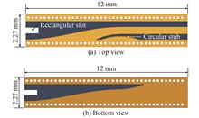
For the convenience of testing, fin-line is used to transform signals from rectangular waveguide to vertical transition structure. Due to the discontinuity between free space and fin-line, a mismatch occurs when free-space waves are transformed into guided waves. A rectangle slot is added at the front end of the structure to match the input impedance. A circular tuning stub is added besides the microstrip-line to extend working bandwidth. The optimized transformation loss is below −1.1 dB and return loss is less than −15 dB in working-band. The structure is constructed on Rogers@ RT4003C with a substrate thickness of 0.203 mm. The fin-line character is shown in the
![]()
Figure 6.Proposed fin-line structure
2 Measurements and results
Vertical transition structure is measured in this section. Performance of the assembled transition structure with the optimum parameters is evaluated by measurement in terahertz band. The measurement was carried out on a Keysight 8257D network analyzer.
![]()
Figure 7.
| Reference | Return loss/dB | Band width/GHz | Insertion loss/dB |
| [ | −15 | 55-65 | −1 |
| [ | −10 | 59-62 | −1.79 |
| This work | −10 | 105-115 | −1.3 |
Table 2. Performance comparisons
3 Conclusion
In this work, a low-loss vertical transition structure for terahertz frequency is demonstrated. The 50-μm thick quartz-substrate with via holes and double-side gold-plated is realized. The estimated transmission loss of the mode-transition structure is −1.3 dB at 110 GHz with an obtained bandwidth of 10 GHz. Combined with a 10 mm thick metal cavity, active circuit can be integrated. The vertical transition structure shows a better performance than that of the cavity-coupled counterparts, exhibiting a more promising prospect in active integrated circuit applications at terahertz frequency.
Acknowledgments
The authors would like to thank Si Liming, Ni Hongbin, Qiao Haidong, Li Mingxun, Guo Dalu (Beijing Institute of Technology) and Xu Zhijun (Han's Laser Technology Group Co., Ltd), for helpful discussions.
References
[5] Li Z, Wang P, Zeng R, et al. Analysis of wideb multilayer LTCC vertical via transition f millimeterwave systeminpackage[C]2017 18th International Conference on Electronic Packaging Technology (ICEPT), IEEE, 2017: 10391042.
[6] Yang L, Zhu L, Choi W W, et al. Novel microstriptomicrostrip vertical transition designed with slotline steppedimpedance resonat[C]2018 International Conference on Microwave Millimeter Wave Technology (ICMMT), IEEE, 2018: 13.
[7] Mozharovskiy A, Churkin S, Arternenko A, et al. Wideb probetype waveguidetomicrostrip transition f 28 GHz applications[C]2018 48th European Microwave Conference (EuMC), IEEE, 2018: 113116.
[9] Tuan N T, Sakakibara K, Kikuma N. Bwidth extension of planar microstriptowaveguide transition by viahole locations at both sides of microstrip line[C]2019 IEEE International Symposium on Antennas Propagation USNCURSI Radio Science Meeting, IEEE, 2019: 673674.
[10] Hosono R, Uemichi Y, Han X, et al. A bwidthenhanced millimeterwave microstrip combline array antenna with parasitic elements on liquid crystal polymer substrate[C]2014 IEEE Antennas Propagation Society International Symposium (APSURSI), 2014: 17261727.

Set citation alerts for the article
Please enter your email address
© Copyright 2018-2021 | Chinese Laser Press. All Rights Reserved 沪ICP备15018463号-20