Han Lin, Qiming Zhang, and Min Gu, "Three-dimensional nanoconfinement of broadband optical energy in all-dielectric photonic nanostructure," Photonics Res. 1, 136 (2013)
Search by keywords or author
- Photonics Research
- Vol. 1, Issue 3, 136 (2013)
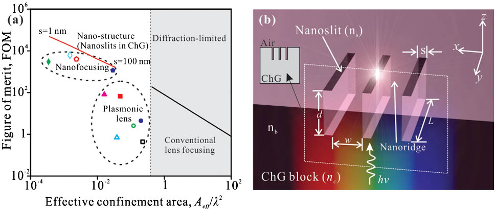
![(a) Plot of the FOM versus the effective confinement area enables a comparison of the nanostructure, optical lens focusing, plasmonic lenses (hollow square [4], solid square [5], hollow circle [6], solid circle [7], hollow triangle [8], solid triangle [8]) and nanofocusing (hollow pentagon [10], solid pentagon [11], hollow diamond [12], solid diamond [13]). The gray area marks the diffraction-limited. The curve of the FOM for the nanostructure is calculated when d=250 nm and s varies in the range from 1 to 100 nm. (b) Schematic of the nanostructure. Three low-index nanoslits are embedded in the high-index ChG block. nc is the refractive index of the ChG block, and ns is the refractive index of the nanoslits. The refractive index of the background is nb. L, s, and d are the length, width, and depth of the nanoslits, respectively. w is the width of the nanoridges. Inset: 2D cross section of the nanostructure.](/richHtml/prj/2013/1/3/03000136/img_001.jpg)
Fig. 1. (a) Plot of the FOM versus the effective confinement area enables a comparison of the nanostructure, optical lens focusing, plasmonic lenses (hollow square [4], solid square [5], hollow circle [6], solid circle [7], hollow triangle [8], solid triangle [8]) and nanofocusing (hollow pentagon [10], solid pentagon [11], hollow diamond [12], solid diamond [13]). The gray area marks the diffraction-limited. The curve of the FOM for the nanostructure is calculated when d = 250 nm s n c n s n b L s d w
![Dependence of (a) effective confinement area Aeff, (b) energy confinement efficiency η, and (c) FOM of the mode on depth d and width s of the nanoslits. The white-dashed line marks the critical transformation length for mode coupling. (d)–(i) x–y and x–z cross sections of the energy density distribution of the nanostructures (d), (e) [s,d]=[100,50] nm, (f), (g) [s,d]=[100,250] nm, and (h), (i) [s,d]=[1,250] nm.](/richHtml/prj/2013/1/3/03000136/img_002.jpg)
Fig. 2. Dependence of (a) effective confinement area A eff η d s x – y x – z [ s , d ] = [ 100 , 50 ] nm [ s , d ] = [ 100,250 ] nm [ s , d ] = [ 1 , 250 ] nm
Fig. 3. Normalized energy density (a) along the x y = 0 z = z f d = 250 nm y x = 0 z = z f d z x = 0 y = 0 s = 1 nm V eff z s d = 250 nm
Fig. 4. (a) Spectral response of the nanostructure ([ s , d ] = [ 1,250 ] nm n c A eff n c η n c
Fig. 5. Normalized energy density at the point of (x = 0 y = 0 z = z f n s [ s , d ] = [ 1 , 250 ] nm n s n c = 2.5 n b = 1

Set citation alerts for the article
Please enter your email address


