
Daoyuan Wang, Dapeng Jin, Peng Zhu, Zhexin Xie, Lei Zeng, Yuliang Zhang, Yongcheng He. Design and implementation of data transmission of fast orbit feedback system for HEPS[J]. High Power Laser and Particle Beams, 2023, 35(7): 074002
- High Power Laser and Particle Beams
- Vol. 35, Issue 7, 074002 (2023)
Abstract
With the enhanced requirements of new synchrotron light sources and the fast development of electronic techniques, the beam orbit stability in μm level can be achieved by the Fast Orbit FeedBack (FOFB) system with a bandwidth of several hundred Hz based on large-volume FPGAs. Low latency is the key to the FOFB system and high-speed serial data transmission techniques provide the perfect solutions with low latency, high data transmission bandwidth and ground isolation between different sub-stations. For HEPS, there are 48 7BAs (seven-bend achromat)[1] with 12 BPMs and 8 fast correctors along the 1360.4 m storage ring[2], 576 BPMs’ data in both horizontal and vertical directions need to be collected and delivered to all of the FOFB sub-stations.
For 3rd generation synchrotron radiation light sources, most of the FOFB systems are based on real-time data transmission links and VME controllers with DSP boards, such as SSRF[3], Diamond[4], SLS[5] and APS[6], with good flexibility and reliability. However, the latency of several hundred μs for these systems cannot fulfill the requirements of tens of μs of the 4th generation light sources. As a 3rd generation light source, NSLS-II[7] has implemented the FOFB system based on FPGAs with RocketIOs[8] and distributed DSPs[9], which shows good performance and has been the preferred choice of the latest high-performance light sources, such as HEPS and APS-U[10].
An FPGA with 80 RocketIOs and 3600 DSPs from Xilinx is chosen for HEPS’s FOFB system due to the overall evaluation of the requirements, the chip performance and the cost.
1 Architecture of data transmission
The fast orbit feedback system is designed to correct the beam orbit in the storage ring with all BPM data as the input and fast correctors’ settings as the output. The feedback method based on the inverse response matrix and PID control is mature and applied widely, thus it is adopted in the implementation of the FOFB system of HEPS.
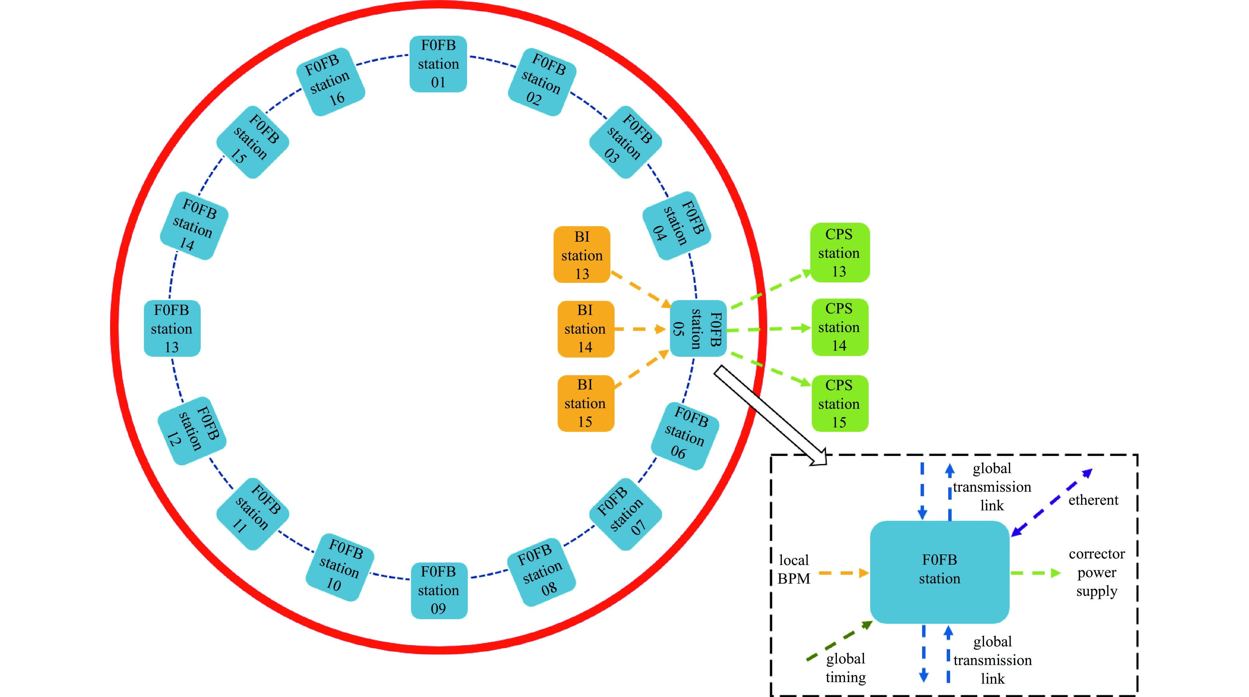
The electronics of the BPMs and the fast correctors of HEPS are located in the 48 Beam Instrumentation (BI) stations on the top of the storage ring due to the lattice design and civil construction[2]. Sub-stations of the FOFB system should be set up since there is no single FPGA chip that can accept all of the BPM channels. To reduce the latency of data transmission of FOFB, the number of sub-stations should be minimized. However, the fewer number of the sub-stations, the more pressure of data processing and calculation for each sub-station. A total of 16 FOFB sub-stations are set up from the 48 BI stations on the top of the storage ring upon the overall evaluation of data transfer latency, civil construction feasibility, connectivity, single FPGA chip capacity and the fraction of number 48.
The 576 BPM channels with two pieces of data transferred by each channel are divided into 16 groups equally, and data is collected by each sub-station with point-to-point connections first, then broadcasted to all of the sub-stations along the ring, as shown in Fig.1. The fast correctors are also divided into 16 groups equally. In total, 36 GTHs (RocketIO named in Vitex7 FPGA manuals) at a line rate of 2.38 Gbps are used in each FOFB sub-station to collect the data from the 36 BPM modules of the 3 BI stations. The global transmission links are bidirectional along the ring to broadcast the BPM data to all sub-stations in only half a ring. The length of the optical fibers between two adjacent sub-stations of FOFB is about 120 m due to the circumference of the ring and the cable routings. A total of 6 GTH channels at a line rate of 4.76 Gbps are used in each sub-station for the global data transmission with 3 GTHs in each direction.
![]()
Figure 1.FOFB architecture of HEPS
A bit width of 32 between the BPM modules and the FOFB sub-stations is used to collect the effective 24-bit signed fixed-point beam position data. The beam-position data is then encoded into 64 bits for global transmission. The 8B/10B encoding is used to reduce the bit error rate during data transmission[8], thus the total transmitted bit width is 40 for the raw beam position data and 80 for the globally encoded beam position data. K28.5 codes are used for the phase alignment in each GTH link.
The 119 MHz clock sourced from the HEPS global timing system is used as the reference for the whole FOFB system. The integer multiples and fractions of the reference clock are used for data transmission and calculation to keep the whole FOFB system synchronized.
The globally encoded BPM data format is shown in Fig.2. Bit [59:49] is the global data coding number, also used as the address of the data in the global memories. The data from each BI station is transferred in group in one of the 3 GTH links and stored in sequence in the global block memories. The group data from each BI station is further divided into two consecutive parts for calculation. Consequently, there are total 96 groups of BPM data with 12 pieces of data in each group. For each group of data, we define the start address as the group address. For each sub-station, the globally encoded BPM data comes from 6 links in both sides concurrently, so the buffers are set for each link. The group addresses are extracted from the global BPM data, according to the group address and the buffer identifier, the write control logic moves the data from the buffers to the global block memories[11] with priority algorithm, the group address is written into the interrupt FIFO[12] at the same time, as shown in Fig.3. The read control logic reads the addresses from the FIFO in sequence, according to which it reads the corresponding data from the global memories to the data calculation pipeline. Lock-protection is designed in the write control logic to avoid inconsistency. A 96-bit register is designed to indicate the successful reception of each group of data.
![]()
Figure 2.Globally encoded BPM data format
![]()
Figure 3.Logic architecture of data encoding and transmission of FOFB
The parameters of inverse response matrix and PID control are also stored in block memories. All the block memories are used in dual-port mode to do writes and reads concurrently. Each group of BPM data and its corresponding parameters are stored in parallel in the block memories and can be read out simultaneously with one clock pulse, as shown in Fig.4.
![]()
Figure 4.Flow chart of HEPS’s FOFB
2 System implementation and test
As illustrated above, the transmission latency is mainly from the local BPM data transmission (T1), the local BPM data encoding (T2), and the global BPM data transmission (T3), as shown in Fig.5.
![]()
Figure 5.Latency of data transmission of FOFB
Due to the overall evaluation of system capability, reliability, availability, scalability and maintainability, the FOFB sub-station is designed as the hardware based on ATCA mechanical architecture with a main logic backplane board, a global timing front board, a global BPM front board, four local BPM front boards, and four fast corrector front boards. As shown in Fig.6, a test station is set up for logic development and system test with the diagram shown in Fig.7. The local BPM data is transferred by 12 channels of a local BPM front board through 30 m OM4 optical fiber loopbacks and received, and the global BPM data is transferred by 3 GTHs through the global BPM front board with 200 m OM4 fiber optic cables and received. The clock units of the backboard[13] provide the synchronous reference clocks of GTHs, and the system clock is generated by the Clock Management Tiles (CMT) of FPGA[14]. Integrated Logic Analyzer (ILA) of FPGA is used to analyze the timing of the data stream by Vivado[15].
![]()
Figure 6.Test station architecture of FOFB
![]()
Figure 7.Test diagram of data transmission of FOFB
The test results show that the latency of local BPM data transmission is 722 ns, according to the system test counter with the counting period of 16.8 ns, and the data are received and written into BRAM with no errors in 24 h, as shown in Fig.8. Considering the field length of 50 m of the OM4 optical fibers between the BI stations and the FOFB sub-station, the latency of local BPM data transmission is estimated as 821 ns with the typical delay of 4.94 ns for 1 m optical fiber[16].
![]()
Figure 8.Latency of local BPM data transmission
The received BPM data are encoded first and then delivered to the global transmission link. The latency of local BPM data encoding is 705 ns, as shown in Fig.9.
![]()
Figure 9.Latency of local BPM data encoding
The latency of global data transmission is 1344 ns, as shown in Fig.10. Considering the field length of 120 m of the OM4 optical fibers between the two adjacent sub-stations, the latency of global BPM data transmission is estimated as 950 ns. No errors occur in global data transmission in 24 h.
![]()
Figure 10.Latency of global BPM data transmission
As Table 1 shows, the total latency of data transmission is estimated less than 10 μs, which can satisfy the requirements on the FOFB system of HEPS.
| T1a/ns | T2b/ns | T3c/ns | (T1+T2+8T3)/ns |
| a The latency of local BPM data transmission, estimated with the length of optical fibers between BI stations and FOFB sub-station
| |||
| 821 | 705 | 950 | 9 126 |
Table 1. Results of data transmission latency
3 Conclusion
A new data transmission architecture based on FPGA for the FOFB system of HEPS is designed and implemented to minimize the latency of data transmission and increase the bandwidth of the system. The data is transferred, collected, delivered and registered with no errors in the test duration of 24 h. A total transmission latency of less than 10 μs is estimated based on the test results and the possible field lengths of optical fibers, which can satisfy the requirements on the FOFB system of HEPS. Further tests with more sub-stations and longer time will be done in the next months to make good preparations for the field installation and joint tests.
References
[3] Jiang Bocheng, Hou J, Yin C X, et al. Status of the SSRF fast bit feedback system[C]Proceedings of IPAC2012. 2012: 28552857.
[4] Uzun I S, Bartolini R, Rehm G, et al. Initial design of the fast bit feedback system f diamond light source[C]Proceedings of the 10th International Conference on Accelerat & Large Experimental Physics Control Systems. 2005.
[5] Schlott V, Böge M, Keil B, et al. Fast orbit feedback and beam stability at the Swiss Light Source[J]. AIP Conference Proceedings, 732, 174-181(2004).
[6] Lipa R, Arnold N, Bui H, et al. APS fast bit feedback system upgrade[C]Proceedings of PAC2013. 2013: 13011303.
[7] Singh O, Bacha B, Blednykh A, et al. NSLSII BPM fast bit feedback system[C]Proceedings of IBIC2013. 2013: 316322.
[8] XILINX. 7 Series FPGAs GTXGTH transceivers user guide[EBOL]. (20180814). https:docs.xilinx.comvuenUSug476_7Series_Transceivers.
[9] XILINX. 7 Series DSP48E1 slice user guide[EBOL]. (20180327). https:docs.xilinx.comvuenUSug479_7Series_DSP48E1.
[10] Bl M, Abliz M, Arnold N, et al. The upgrade of the advanced photon source[C]Proceedings of the 9th International Particle Accelerat Conference. 2018: 28722877.
[11] XILINX. 7 Series FPGAs memy resources user guide[EBOL]. (20190703). https:docs.xilinx.comvuenUSug473_7Series_Memy_Resources.
[12] XILINX. FIFO generat v13.2 LogiCE IP product guide[EBOL]. (20171004). https:docs.xilinx.comvuenUSpg057fifogenerat.
[13] Zhu P, Jin D P, Zhang Y L, et al. The status of fast obit feedback system of HEPS[C]Proceedings of the 18th International Conference on Accelerat & Large Experimental Physics Control Systems. 2021: 540543.
[14] XILINX. 7 Series FPGAs clocking resources user guide[EBOL]. (20180730). https:docs.xilinx.comvuenUSug472_7Series_Clocking.
[15] XILINX. Integrated logic analyzer v6.2 LogiCE IP product guide[EBOL]. (20161005). https:docs.xilinx.comvuenUSpg172ila.
[16] Huang Rong, Wang Runhan, Xiao Wufeng, et al. Transmission perfmance of OM3, OM4, OM5 multimode fibers[C]Proceedings of SPIE 11048, 17th International Conference on Optical Communications wks (ICOCN2018). 2019: 110483M.

Set citation alerts for the article
Please enter your email address
© Copyright 2018-2021 | Chinese Laser Press. All Rights Reserved 沪ICP备15018463号-20