
Jie Yan, Miao-Miao Wei, Yan-Xia Xing. Dephasing effect of quantum spin topological states in HgTe/CdTe quantum well [J]. Acta Physica Sinica, 2019, 68(22): 227301-1
- Acta Physica Sinica
- Vol. 68, Issue 22, 227301-1 (2019)
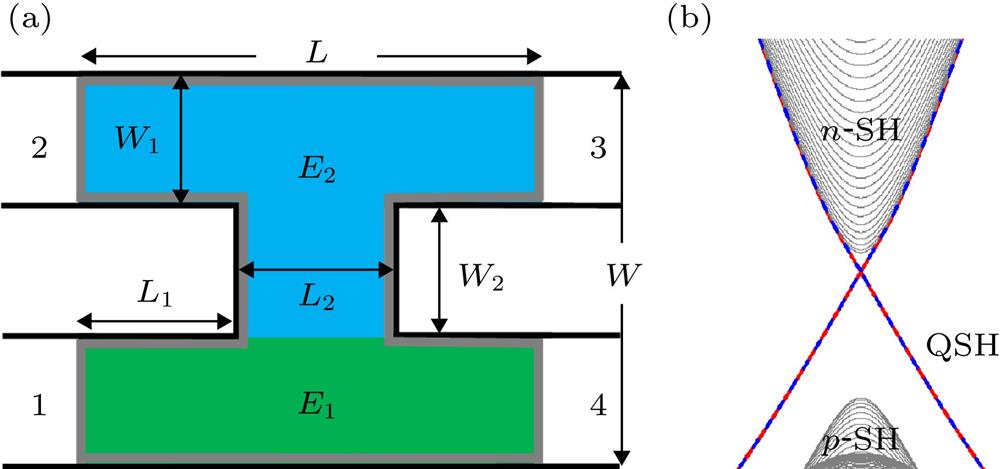
Fig. 1. (a) Four-terminal device based on HgTe/CdTe quantum well with two current terminals 1, 4 and two voltage terminals 2, 3; the blue region and green region can be independently tuned into the three region shown in panel (b); (b) band structure of 2 D HgTe/CdTe quantum well. Bulk energy gap divides three region: QSH region, n-SH region and p-SH region.(a) 四端口HgTe/CdTe量子阱模型, 其中1、4端口为电流输入端口, 2、3端口为电压测量端口. 图中蓝色和绿色区域分别由两个独立的门电压控制, 通过调节门电压, 两个区域可分别独立地在图(b)中所示的三个区间自由切换; (b) HgTe/CdTe量子阱二维系统的能带结构, 包含简并的螺旋边缘态和明显不对称的价带和导带. 体带隙分割出三个区域: 量子自旋霍尔区(QSH), n型自旋霍尔区(n-SH)和p型自旋霍尔区(n-SH)
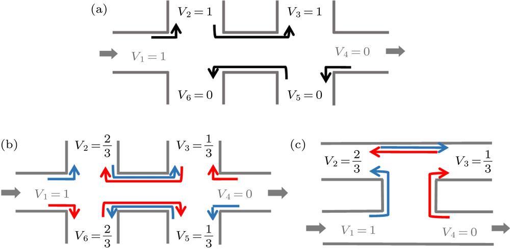
Fig. 2. Sketch map of voltage drop induced by chiral edge states and helical edge states in multi-terminal system.手性边缘态和螺旋边缘态在多端口体系中的电压降示意图
Fig. 3. Nonlocal resistors
and transmission coefficient
and
vs energy
with energy of detector region
. left and right panels are for
and
, respectively. Top panels are band structure of infinite ribbon, the blue lines and red lines correspond to spin up and spin down, respectively.
纵向非局域电阻
和部分透射系数
和
随电流输入区(图1 绿色区)在位能
的变化. 左右两栏分别对应铁磁交换场
和
的情况, 探测区(图1 蓝色区)在位能
. 为便于比较, 顶栏给出了相应能量区间的能带图. 能带图中, 蓝色和红色分别表示自旋上和自旋下的能带
Fig. 4. Panel (a)
vs energy
. Panel (b) and (c): longitudinal non-local resistance
vs energy
with different
for normal dephasing [panel (b)] and spin dephasing [panel (c)].
(a)不同退相干条件下
随费米能的变化; (b)和(c): 在普通退相干(图(b))和自旋退相干(图(c))作用下, 纵向非局域电阻
随入射端能量
的变化, 不同曲线对应不同的退相干强度. 图(b)和图(c)共享图例
Fig. 5. Band structures of infinite ribbon with various magnetic field B for exchange field
(top panels) and
(bottom panels). Red lines denotes the chiral edge states. The red lines and blue lines are correspond to the states of spin up and spin down.
磁场从弱到强作用下无穷长条带在零磁交换场(上栏)和非零磁交换场(下栏)条件下的能带演化
Fig. 6. Schematic diagram of the developing tendency of band structure in the presence of magnetic field for the zero exchange field (top panels) and nonzero exchange field (bottom panels).零磁交换场和非零磁交换场能带随外磁场的演化趋势示意图
Fig. 7. vs energy
for different normal dephasing strength
with (right panels) or without (left panels) exchange field. The gray region signs the energy gap in zero magnetic field.
普通退相干和磁场作用下, 纵向非局域电阻
随入射端能量
的变化. 左栏: 零磁交换场; 右栏: 非零磁交换场. 上下两栏共享图例
Fig. 8. vs energy
, the dephasing precesses are spin non-conserved. The other parameters are the same as Fig. 7 自旋退相干作用下的纵向非局域电阻, 其余参数设置同图7

Set citation alerts for the article
Please enter your email address
© Copyright 2018-2021 | Chinese Laser Press. All Rights Reserved 沪ICP备15018463号-20