Abstract
We propose and experimentally demonstrate a novel ultracompact dual-mode waveguide crossing based on subwavelength multimode-interference couplers for a densely integrated on-chip mode-division multiplexing system. By engineering the lateral-cladding material index and manipulating phase profiles of light at the nanoscale using an improved inverse design method, a subwavelength structure could theoretically realize the identical beat length for both and , which can reduce the scale of the device greatly. The fabricated device occupied a footprint of only . The measured insertion losses and crosstalks were less than 0.6 dB and from 1530 nm to 1590 nm for both and modes, respectively. Furthermore, our scheme could also be expanded to design waveguide crossings that support more modes.1. INTRODUCTION
Recently, mode-division multiplexing (MDM) on a silicon-on-insulator (SOI) platform, as a more promising and attractive technology, provides an effective approach to further increase the transmission spectral efficiency and capacity of an on-chip optical interconnect [1]. To realize an MDM system, various key building blocks have been extensively reported, e.g., mode (de)multiplexers [(DE)MUX] [2–6], mode switches [7,8], and multimode bent waveguides [9,10]. A high-performance multimode waveguide crossing with compact footprint, low insertion loss (IL), and low crosstalk (CT), which is an essential component for realizing a densely integrated MDM optical network, has been rarely addressed considering the complex mode coupling in the crossing region for high order modes. Recently, the self-image effect of conventional multimode-interference (MMI) couplers has been utilized to realize the dual-mode waveguide crossing [11]. Unfortunately, the severe self-image position offset between the fundamental transverse magnetic modes () and first-order transverse magnetic modes () in a conventional waveguide leads to a relatively large coupling length and complicated design process. Therefore, one may use a symmetric Y-junction to convert high order modes to the fundamental modes to relax the subsequent processing [12]. However, the additional symmetric Y-junction might inevitably increase the insertion loss and scale of the device. A multimode waveguide crossing with a compact footprint and excellent performance is still highly desired for a densely integrated MDM optical network.
Due to the capability of flexible refractive index engineering at the subwavelength (SW) scale, subwavelength gratings (SWGs) have been utilized to realize waveguide crossings, broadband directional couplers, and fiber-to-chip couplers [13–16]. On the other hand, free-form silicon SW structures based on inverse design methods also provide an alternative approach to engineer the refraction index at the nanoscale and have shown great potential to realize ultracompact and highly functional devices simultaneously [17–19]. However, the random and complex etching patterns in these structures may inevitably introduce large fabrication errors. To resolve this issue, we earlier proposed a fabrication-error-insensitive subwavelength structure, i.e., the PhC-like SW structure, to suppress fabrication errors caused by the lag effect of the plasma etching process [20]. Moreover, inverse designs of SW-structure devices are usually nonsmooth optimization problems. Different initial patterns probably lead to different local-optimum patterns using the same iteration algorithm. One has to use many random initial patterns to generate many “optimized” patterns and then select a relatively “best” one as the device pattern. It is disadvantageous for improving design efficiency and device performance.
In this work, we propose a novel ultracompact dual-mode waveguide crossing composed of a PhC-like SW-based MMI coupler using an improved inverse design method. We theoretically analyze the feasibility of designing a subwavelength MMI coupler with perfect self-image beat-length matching between the two modes based on regular PhC-like subwavelength waveguides. To improve the design efficiency and device performance, we propose to choose a manually set pattern based on a predesigned subwavelength MMI coupler, instead of a random one, as the initial pattern to start the optimization process of inverse design. In this way, the footprint of the proposed device is reduced by one order of magnitude smaller than that of conventional waveguide-based MMI couplers. Simulation results also show that the performance of the optimized device based on an MMI-like initial pattern is significantly improved compared with other optimized devices based on random initial patterns. The fabricated dual-mode waveguide crossing occupied , which may be the most compact dual-mode waveguide crossing that has been reported to the best of our knowledge. The measured insertion losses and crosstalk for both and were less than 0.6 dB and over an operating bandwidth of 60 nm centered at 1560 nm, respectively.
Sign up for Photonics Research TOC. Get the latest issue of Photonics Research delivered right to you!Sign up now
2. DESIGN, OPTIMIZATION, AND SIMULATIONS
The operation principle of the dual-mode waveguide crossing is illustrated in Fig. 1(a), where the -fold images of the and launched into the input waveguide can be formed at the center of the intersection regions. The proposed structure is composed of two vertically crossed MMI couplers and the lateral claddings. and are the material refractive indices of MMI couplers and the lateral claddings, respectively. Due to the axisymmetric structure, the injected could only excite and , while the injected could only excite and similarly. According to the self-imaging effect of multimode interference, the -fold images of the and could be periodically formed at the integer times of the corresponding beat lengths. The beat lengths for the two modes in MMI couplers are defined as [21,22] where is the beat length of the mode launched in the input waveguide. and are the propagation constants of the excited and in the MMI region, respectively. The primary target for the dual-mode waveguide crossing design is to find the proper MMI length to realize perfect self-images for both modes simultaneously. To minimize the footprint of MMI couplers, should be the same as . However, as is presented in Fig. 1(b), an offset between and is inevitable for conventional waveguide-based MMI. In order to realize the perfect self-images for both modes, a typical method is to set as the least common multiple of and , leading to a large footprint device [11].
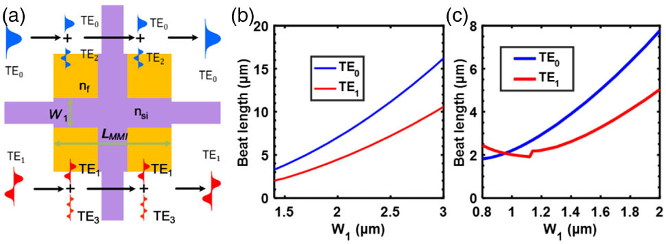
Figure 1.(a) Schematic illustration of the dual-mode waveguide crossing. (b) and (c) Self-image beat lengths of both modes for the conventional waveguide-based MMI coupler and SW-structure-assisted one as a function of , respectively.
On the other hand, a PhC-like SW structure could provide an additional design degree of freedom to optimize the self-image lengths for individual modes. By engineering the refractive indices of the lateral claddings and changing the widths of MMI couplers, we could flexibly optimize self-image lengths for both modes. Considering the proposed PhC-like SW structure in our previous work [20], here, of PhC-like SW-based lateral claddings is set as 2.38. As shown in Fig. 1(c), the same self-image beat lengths of both modes for SW-assisted MMI couplers could be expected to be achieved theoretically. and are about 0.96 μm and 2 μm, respectively. In addition, free-form PhC-like SW structures could also manipulate the phase profiles of the excited multimodes in the MMI region with a high degree of freedom at the nanoscale [23], which is utilized to minimize the modal mismatch between input waveguide and SW-assisted MMI couplers and the modal phase errors in MMI couplers. In this way, an ultracompact and highly functional dual-mode waveguide crossings could be achieved simultaneously.
As shown in Fig. 2(a), the proposed dual-mode waveguide crossing based on PhC-like SW is designed on an SOI platform with a 220 nm thick air-cladded top silicon layer. The device consists of two vertically crossed multimode-interference couplers and a fourfold symmetric inverse design region. The widths of two MMI couplers are set as 900 nm to support both and . As described in the previous discussion, the length of in our proposed device should be . In order to further suppress the modal mismatch between the input waveguide and SW-assisted MMI couplers, the additional taper section in the inverse design region should be considered. As a result, in our proposed device is predesigned as 4.8 μm. Therefore, the inverse design region composed of discrete pixels occupies a compact footprint of , which is more than one order of magnitude smaller than that of the conventional one. The size of each pixel is and the shape of each pixel is a square with a circular hole at its center. The hole has a radius of 45 nm and a depth of 220 nm. Based on the effective medium theory [24], the effective material refractive index of our proposed PhC-like SW with an air hole is 2.38 at the wavelength of 1.55 μm. Each pixel has only two states: “0” denotes the hole is fully etched, while “1” denotes the hole is not etched, where the 220 nm thick silicon remains. Due to the fourfold symmetry of the proposed device, we only need to take one half-quadrant with 210 independent pixels into consideration. The goal of the optimized design is to obtain the optimized circular hole combinations in the inverse design region to realize the perfect self-images for both modes.

Figure 2.(a) Schematic of the dual-mode crossings based on SW-structure MMI couplers. (b)–(e) Manually set and random initial patterns. (f)–(i) Optimized patterns for the manually set and random initials. (j) Calculated FOMs after every iteration for the manual and random initial patterns. (k) and (l) Transmission spectra for and of the four optimized devices with different initial patterns, respectively.
It is well known that the inverse design optimization algorithm is usually sensitive to the initial patterns. To achieve a better performance device, we manually set an MMI-like initial pattern rather than a random one to start the searching process of inverse design, as shown in Fig. 2(b). As described in previous discussion, the width of the optimized MMI couplers should be about 0.96 μm. Therefore, to easily realize the identical beat lengths for both modes, the states of the corresponding eight lines of holes within optimized MMI couplers should be set to be “1.” In addition, to verify the reasonability and validity of our equivalent model, we also design three random initial patterns for comparison and analysis, as shown in Figs. 2(c)–2(e). Our following simulation results indicate that the device with a manually set MMI-like initial pattern usually exhibits better performance than those with random ones. The figure-of-merit (FOM) in our optimization process is defined as where and are the transmittance of and injected in the input waveguide via inverse design region, respectively. Likewise, denotes the number of wavelength channels, and three wavelengths over an operating bandwidth of 80 nm are taken into consideration in simulations. For an ideal dual-mode waveguide crossing, the calculated FOM should be equal to 1.
The nonlinear direct-binary-search (DBS) optimization algorithm is employed to design the local optimum pattern [18]. A 3D finite-difference time-domain (FDTD) method is used to calculate the FOM via commercial software (Lumerical FDTD Solutions) [25]. At the beginning of the optimization process, we randomly choose one pixel to toggle its state and calculate the FOM. If the FOM is improved, the reversed pixel state will be reserved. Otherwise, the pixel will be toggled to the original state. One iteration ends up with all pixels traversed. And the whole optimization will end up with the FOM exhibiting no greater improvement after one iteration ( for our case). It takes about 24 h to obtain the optimized nanopattern after six rounds of iteration on a computer with an eight-core central processing unit (Intel Xeon E5-2637).
The optimized patterns based on the manually set MMI-like initial pattern and the randomly generated ones with the same optimization process are presented in Figs. 2(f)–2(i), respectively. The calculated FOMs for all the patterns after six rounds of iteration are also illustrated in Fig. 2(j). The corresponding transmission spectra for and of the four optimized devices with different initial patterns are shown in Figs. 2(k) and 2(l), respectively. As expected, the FOMs and ILs for both modes for the manually set MMI-like initial pattern are usually better than those for the random ones, which indicates that an MMI-like initial pattern may provide an effective approach to achieve higher performance.
Three-dimensional FDTD simulation results are utilized to evaluate the performance of the optimized PhC-like SW structure-assisted MMI dual-mode waveguide crossing. The magnetic field distributions of Hz at 1550 nm for and are illustrated in Figs. 3(a) and 3(b), respectively. As we can see, the working mechanism of the inverse designed nanophotonic device is equivalent to that of the SW structure-assisted MMI dual-mode waveguide crossing. Both and have the same beat lengths to realize the self-images at the center of MMI couplers, which could reduce the scale by one order of magnitude smaller than that based on conventional waveguide MMI couplers. A PhC-like SW structure also provides an effective approach to manipulate the phase profiles of an optical field at the nanoscale to further suppress the modal phase errors introduced in the excited modes. Therefore, an approximately perfect self-image might be achieved in our simulations. The transmittances and CTs as a function of wavelength for and launched in the input waveguide are presented in Figs. 3(c) and 3(d), respectively. The simulated ILs for both and are less than 0.5 dB, and the CTs at the cross port are lower than from 1520 to 1600 nm, respectively. Notably, due to the symmetric structure in our proposed device, the antisymmetric mode () at the bar port could not theoretically be excited by the symmetric mode () injected in the input port. Likewise, at the bar port could also not be excited by . Therefore, the CTs less than for both modes at the bar port are negligible, which are not shown in Figs. 3(c) and 3(d).
Figure 3.(a) and (b) Simulated magnetic field distributions of Hz for and at the wavelength of 1560 nm, respectively. (c) and (d) Simulated transmission spectra for and , respectively.
3. EXPERIMENT RESULTS
The proposed ultracompact dual-mode waveguide crossing based on the PhC-like SW structure MMI couplers was fabricated and experimentally demonstrated. First, an electron-beam lithography system (Vistec EBPG 5000 Plus) was used to form the optimized pattern on SOI platform with a 220 nm thick top silicon layer. After that, an inductively coupled plasma etcher (Plasma lab System100) was utilized to transfer the mask to the silicon device layer. Despite the lag effect, we can actually ensure the nanopattern to be fully etched through increasing the etching time [26]. The SW structure asymmetrical Y-junction-based MUX was utilized to excite the higher order modes [26]. Besides, an extra reference MDM system was also fabricated to evaluate the performance of the device.
Figure 4(a) shows the top-view scanning electron microscope (SEM) picture of the fabricated device composed of a dual-mode waveguide crossing, MUX, and DEMUX. Figure 4(b) shows the reference MDM system. The detailed SEM images of the fabricated dual-mode waveguide crossing and MUX are illustrated in Figs. 4(c) and 4(d), respectively. A broad amplified spontaneous emission light source and an optical spectrum analyzer (Yokogawa AQ6370C-20) were utilized to measure the spectral transmission. From the spectral transmission scans for each combination of input and output ports, the performance of the reference MDM system was characterized [as illustrated in Fig. 4(e)], in which, for example, “1–2” denotes the spectral transmission from input port 1 (I1) to output port 2 (O2). and are excited when the light is launched in input port I1 and I2, respectively. The measured average ILs were less than 1 dB, and the CTs were lower than for both and from 1.53 to 1.59 μm. Similarly, spectral transmission of the entire device composed of the proposed crossing and two MUXs or DEMUXs was measured and characterized, as shown in Fig. 4(f). The measured average ILs for both and modes were less than 1.6 dB. That means that the average ILs of our fabricated crossing should be less than 0.6 dB. The measured CTs for both modes at the bar port and the cross port were less than and , respectively. To our best knowledge, our dual-mode crossing only occupied a footprint of , which is the most compact scale. The proposed scheme would show great potential in a densely integrated MDM system for an on-chip optical interconnect.
Figure 4.(a) SEM image for the fabricated device composed of a dual-mode waveguide crossing and four (DE)MUXs. (b) SEM picture for the reference MDM system. (c) and (d) Detailed SEM images for dual-mode waveguide crossing and MUX. (e) and (f) Normalized measured transmission spectra for the fabricated reference MDM link and the entire fabricated device consisting of our proposed crossing and a pair of (DE)MUXs, respectively.
To further verify the ILs for both modes and suppress measurement errors introduced by the MDM system, we designed, fabricated, and experimentally characterized three, five, seven, and 10 cascaded crossings. The measured ILs for the and modes are shown in Figs. 5(a) and 5(b), respectively. Due to reflection between the conventional bus multimode waveguide and SW structure MMI-based crossings in the periodical cascaded structures, the Fabry–Perot resonances were formed in the fabricated devices. The length of cavity, including bus multimode waveguide and the proposed crossing, is 8.8 μm. The interval between the neighboring Fabry–Perot resonances around 1550 nm is approximately 34 nm, as given in Fig. 5(a). Due to the effective Fabry–Perot cavity length of 8.8 μm, the interval is theoretically calculated to be 34.1 nm, which agrees well with our measured one. Figures 5(c) and 5(d) show the normalized transmission as a function of the cascaded crossings number for and , respectively. The average ILs for and obtained from the slope of linear fitting plots are 0.43 and 0.41 dB per crossing at the wavelength of 1560 nm, respectively. Meanwhile, the measured average ILs for both modes were less than 0.53 dB over an operating bandwidth of 80 nm centered at 1560 nm. We believe our proposed device with its compact footprint and low ILs will show great potential in densely integrated photonic circuit applications.
Figure 5.(a) and (b) Measured transmission spectra with different numbers of cascaded crossings for and , respectively. (c) and (d) Measured ILs at 1560 nm as a function of cascaded crossing numbers for and , respectively.
4. CONCLUSION
In summary, we have proposed and experimentally demonstrated an ultracompact dual-mode waveguide crossing based on PhC-like SW-structure-assisted MMI using the inverse design method. A PhC-like SW structure provides additional freedom to suppress the offset of beat lengths for and in a conventional waveguide, due to engineering material index and manipulating phase profiles of light at the nanoscale. Therefore, both and could realize a self-image simultaneously in several micrometers, which can decrease the footprint greatly. The fabricated dual-mode crossing occupied , which is more than one order of magnitude smaller than that of a conventional one. Besides, our simulation results indicate that the MMI-like initial pattern designed by the well-known conventional model helps us to achieve better performance than a random one does. The measured ILs for both and modes were less than 0.6 dB, and the measured CTs at the bar and cross port were lower than and from 1530 to 1590 nm, respectively. In addition, to suppress measurement errors, the cascaded crossings were also designed and fabricated. The average measured ILs for and were 0.41 and 0.43 dB per crossing at 1560 nm, respectively, which agree with our simulations. Furthermore, our proposed scheme could be expanded to design multimode crossings supporting more modes. The proposed dual-mode waveguide crossings may offer an attractive approach to promote practical applications of densely integrated photonic MDM systems for on-chip optical interconnections. Finally, the improved inverse design method based on a well-known conventional waveguide model could be applied to inversely design different types of nanophotonic devices if we can predesign the initial patterns based on proper conventional models.
References
[1] D. Dai, J. E. Bowers. Silicon-based on-chip multiplexing technologies and devices for peta-bit optical interconnects. Nanophotonics, 3, 283-311(2014).
[2] J. Wang, S. He, D. Dai. On-chip silicon 8-channel hybrid (de)multiplexer enabling simultaneous mode- and polarization-division multiplexing. Laser Photon. Rev., 8, L18-L22(2014).
[3] J. Wang, P. Chen, S. Chen, Y. Shi, D. Dai. Improved 8-channel silicon mode demultiplexer with grating polarizers. Opt. Express, 22, 12799-12807(2014).
[4] Y. Ding, J. Xu, F. Da Ros, B. Huang, H. Ou, C. Peucheret. On-chip two-mode division multiplexing using tapered directional coupler-based mode multiplexer and demultiplexer. Opt. Express, 21, 10376-10382(2013).
[5] L. Luo, N. Ophir, C. P. Chen, L. H. Gabrielli, C. B. Poitras, K. Bergmen, M. Lipson. WDM-compatible mode-division multiplexing on a silicon chip. Nat. Commun., 5, 3069-3075(2014).
[6] J. B. Driscoll, R. R. Grote, B. Souhan, J. I. Dadap, M. Lu, R. M. Osgood. Asymmetric Y junctions in silicon waveguides for on-chip mode-division multiplexing. Opt. Lett., 38, 1854-1856(2013).
[7] Y. Zhang, Y. He, Q. Zhu, C. Qiu, Y. Su. On-chip silicon photonic 2 × 2 mode- and polarization-selective switch with low inter-modal crosstalk. Photon. Res., 5, 521-526(2017).
[8] Y. Xiong, R. B. Priti, O. Liboiron-Ladouceur. High-speed two-mode switch for mode-division multiplexing optical networks. Optica, 4, 1098-1102(2017).
[9] L. H. Gabrielli, D. Liu, S. G. Johnson, M. Lipson. On-chip transformation optics for multimode waveguide bends. Nat. Commun., 3, 1217-1232(2012).
[10] C. Sun, Y. Yu, G. Chen, X. Zhang. Ultra-compact bent multimode silicon waveguide with ultralow inter-mode crosstalk. Opt. Lett., 42, 3004-3007(2017).
[11] H. Xu, Y. Shi. Dual-mode waveguide crossing utilizing taper-assisted multimode-interference couplers. Opt. Lett., 41, 5381-5384(2016).
[12] C. Sun, Y. Yu, X. Zhang. Ultra-compact waveguide crossing for a mode-division multiplexing optical network. Opt. Lett., 42, 4913-4916(2017).
[13] P. J. Bock, P. Cheben, J. H. Schmid, J. Lapointe, A. Delâge, D.-X. Xu, S. Janz, A. Densmore, T. J. Hall. Subwavelength grating crossings for silicon wire waveguides. Opt. Express, 18, 16146-16155(2010).
[14] A. Maese-Novo, R. Halir, S. Romero-Garcia, D. Perez-Galacho, L. Zavargo-Peche, A. Ortega-Monux, I. Molina-Fernandez, J. G. Wangueemert-Perez, P. Cheben. Wavelength independent multimode interference coupler. Opt. Express, 21, 7033-7040(2013).
[15] D. Benedikovic, P. Cheben, J. H. Schmid, D. Xu, B. Lamontagne, S. Wang, J. Lapointe, R. Halir, A. Ortega-Moñux, S. Janz, M. Dado. Subwavelength index engineered surface grating coupler with sub-decibel efficiency for 220-nm silicon-on-insulator waveguides. Opt. Express, 23, 22628-22635(2015).
[16] Y. Wang, W. Shi, X. Wang, Z. Lu, M. Caverley, R. Bojko, L. Chrostowski, N. A. Jaeger. Design of broadband subwavelength grating couplers with low back reflection. Opt. Lett., 40, 4647-4650(2015).
[17] A. Y. Piggott, J. Lu, K. G. Lagoudakis, J. Petykiewicz, T. M. Babinec, J. Vučković. Inverse design and demonstration of a compact and broadband on-chip wavelength demultiplexer. Nat. Photonics, 9, 374-377(2015).
[18] B. Shen, P. Wang, R. Polson, R. Menon. An integrated-nanophotonics polarization beam splitter with footprint. Nat. Photonics, 9, 378-382(2015).
[19] A. Y. Piggott, J. Lu, T. M. Babinec, K. G. Lagoudakis, J. Petykiewicz, J. Vučković. Inverse design and implementation of a wavelength demultiplexing grating coupler. Sci. Rep., 4, 7210-7214(2015).
[20] L. Lu, D. Liu, F. Zhou, D. Li, M. Cheng, L. Deng, S. Fu, J. Xia, M. Zhang. Inverse-designed single-step etched colorless 3 dB couplers based on RIE-lag-insensitive PhC-like subwavelength structures. Opt. Lett., 41, 5051-5054(2016).
[21] L. B. Soldano, E. C. Pennings. Optical multi-mode interference devices based on self-imaging: principles and applications. J. Lightwave Technol., 13, 615-627(1995).
[22] C. Chen, C. Chiu. Taper-integrated multimode-interference based waveguide crossing design. IEEE J. Quantum Electron., 46, 1656-1661(2010).
[23] L. Lu, M. Zhang, F. Zhou, W. Chang, J. Tang, D. Li, D. Liu. Inverse-designed ultra-compact star-crossings based on PhC-like subwavelength structures for optical intercross connect. Opt. Express, 25, 18355-18364(2017).
[24] L. Lalanne, D. Lemercier-Lalanne. On the effective medium theory of subwavelength periodic structures. J. Mod. Opt., 43, 2063-2085(1996).
[25] Lumerical FDTD.
[26] W. Chang, L. Lu, X. Ren, D. Li, Z. Pan, M. Cheng, D. Liu, M. Zhang. Ultra-compact mode (de)multiplexer based on subwavelength asymmetric Y-junction. Opt. Express, 26, 8162-8170(2018).

