• Acta Photonica Sinica
  • Vol. 51, Issue 6, 0623003 (2022)
Jiashun ZHANG1、2, Junming AN2、*, Bingli SUN3, Jun CHEN3, Yanzhang HU3, and Chongxin SHAN1
Author Affiliations
  • 1Henan Diamond Optoelectronic Materials and Devices Key Laboratory,School of Physics and Engineering,Zhengzhou University,Zhengzhou 450001,China
  • 2State Key Laboratory of Integrated Optoelectronics,Institute of Semiconductors,Chinese Academy of Sciences,Beijing 100083,China
  • 3Henan Key Laboratory of Optoelectronic Circuit and Integration,Henan Shi Jia Photons Technology Co.,Ltd,Hebi,Henan 458030,China
  • show less
    DOI: 10.3788/gzxb20225106.0623003 Cite this Article
    Jiashun ZHANG, Junming AN, Bingli SUN, Jun CHEN, Yanzhang HU, Chongxin SHAN. Fabrication of Silica Based Silicon 20 Channel Cyclic Arrayed Waveguide Grating[J]. Acta Photonica Sinica, 2022, 51(6): 0623003 Copy Citation Text show less
    Schematic structure of arrayed waveguide grating
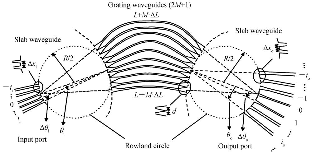
    Fig. 1. Schematic structure of arrayed waveguide grating
    The diagram of 1×20 cyclic AWG
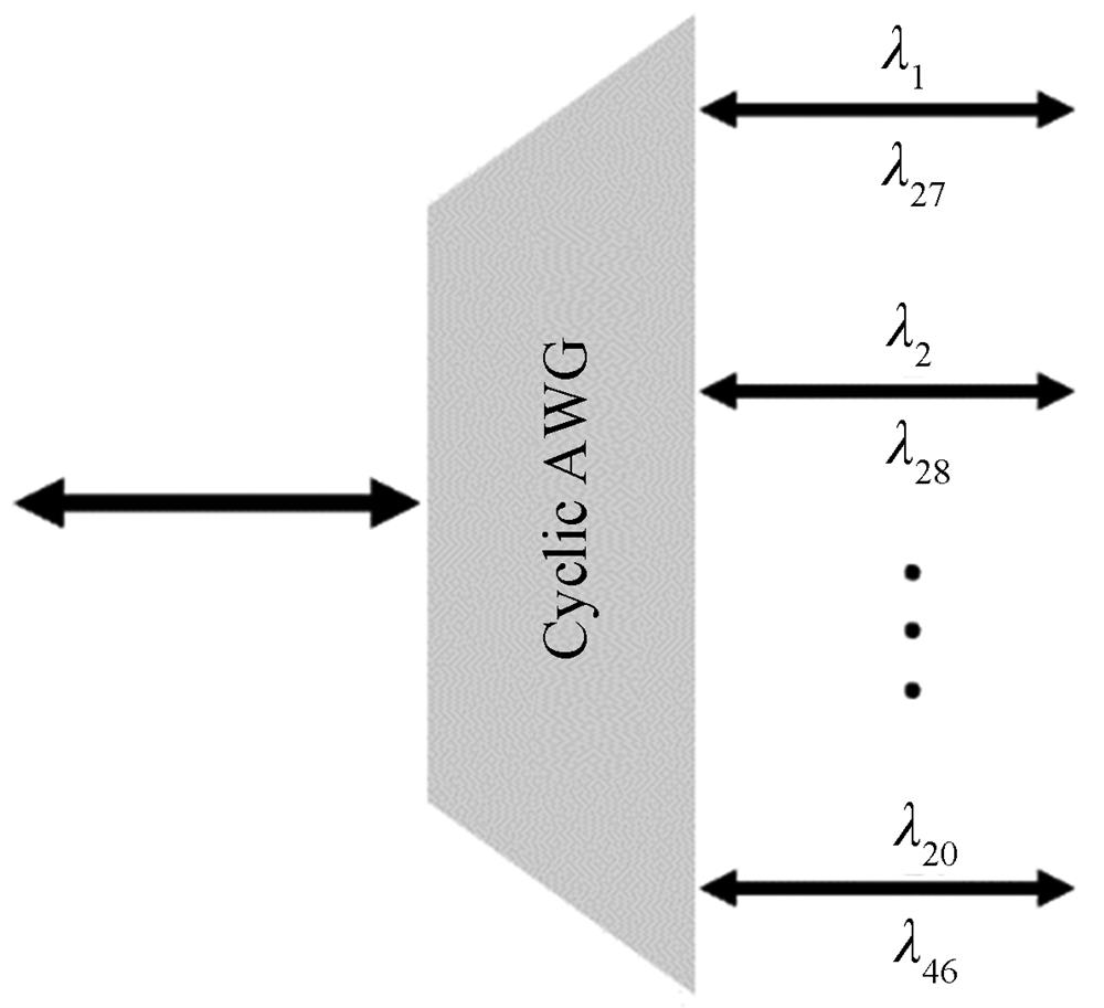
    Fig. 2. The diagram of 1×20 cyclic AWG
    The diagram of 2×20 cyclic AWG
    Fig. 3. The diagram of 2×20 cyclic AWG
    Schematic structure of input waveguide
    Fig. 4. Schematic structure of input waveguide
    Simulated spectra of different exponential tapered waveguide widths
    Fig. 5. Simulated spectra of different exponential tapered waveguide widths
    Simulated spectra of 1×20 cyclic AWG
    Fig. 6. Simulated spectra of 1×20 cyclic AWG
    Center wavelength offset of 1×20 cyclic AWG
    Fig. 7. Center wavelength offset of 1×20 cyclic AWG
    Simulated spectra of 2×20 cyclic AWG
    Fig. 8. Simulated spectra of 2×20 cyclic AWG
    Center wavelength offset of 2×20 cyclic AWG
    Fig. 9. Center wavelength offset of 2×20 cyclic AWG
    The layout of 2×20 cyclic AWG
    Fig. 10. The layout of 2×20 cyclic AWG
    AWG microscope photo and cross section SEM photo
    Fig. 11. AWG microscope photo and cross section SEM photo
    Photo of 20 channel cyclic AWG athermal module
    Fig. 12. Photo of 20 channel cyclic AWG athermal module
    Test spectrum of 20 channel cyclic AWG athermal module
    Fig. 13. Test spectrum of 20 channel cyclic AWG athermal module
    Test center wavelength offset of 20 channel cyclic AWG athermal module
    Fig. 14. Test center wavelength offset of 20 channel cyclic AWG athermal module
    Channel

    HE→TE

    /THz

    TE→HE

    /THz

    Channel

    HE→TE

    /THz

    TE→HE

    /THz

    Ch20(λ2046194.1191.5Ch10(λ1036195.1192.5
    Ch19(λ1945194.2191.6Ch9(λ935195.2192.6
    Ch18(λ1844194.3191.7Ch8(λ834195.3192.7
    Ch17(λ1743194.4191.8Ch7(λ733195.4192.8
    Ch16(λ1642194.5191.9Ch6(λ632195.5192.9
    Ch15(λ1541194.6192.0Ch5(λ531195.6193.0
    Ch14(λ1440194.7192.1Ch4(λ430195.7193.1
    Ch13(λ1339194.8192.2Ch3(λ329195.8193.2
    Ch12(λ1238194.9192.3Ch2(λ228195.9193.3
    Ch11(λ11/λ37195.0192.4Ch1(λ127196.0193.4
    Table 1. 20 Ch WDM system center frequency
    ParameterValue
    Diffraction order m74
    Roland circle diameter R /μm5 390.101
    Length difference ΔL /μm78.381 244 3
    Wavelength spacing ∆λ /nm0.788
    Input/Output waveguide spacing ∆xo /μm22
    Array waveguide spacing d /μm10
    No. of array waveguides151
    Input taper width /μm22
    Output taper width /μm10
    Array waveguide taper width /μm9
    Center wavelength λ0 /nm1 536.61
    Table 2. Design geometric parameters of 1×20 cyclic AWG
    ParameterValue
    Diffraction order m37
    Roland circle diameter R /μm10 780.202
    Length difference ΔL /μm38.935 596 03
    Wavelength spacing ∆λ /nm0.788
    Input/Output waveguide spacing ∆xo /μm22
    Array waveguide spacing d /μm10
    No. of array waveguides301
    Input taper width /μm22
    Output taper width /μm10
    Array waveguide taper width /μm9
    Center wavelength λ0 /nm1 526.61
    Table 3. Design geometric parameters of 2×20 cyclic AWG
    Jiashun ZHANG, Junming AN, Bingli SUN, Jun CHEN, Yanzhang HU, Chongxin SHAN. Fabrication of Silica Based Silicon 20 Channel Cyclic Arrayed Waveguide Grating[J]. Acta Photonica Sinica, 2022, 51(6): 0623003
    Download Citation