• Chinese Physics B
  • Vol. 29, Issue 8, (2020)
Wei-Qi Huang1、2、†, Shi-Rong Liu3, Hong-Yan Peng1, Xin Li2, and Zhong-Mei Huang2
Author Affiliations
  • 1Department of Physics, Hainan Normal University, Haikou 5758, China
  • 2Institute of Nanophotonic Physics, Guizhou University, Guiyang 55005, China
  • 3State Key Laboratory of Environment Geochemistry, Institute of Geochemistry, Chinese Academy of Sciences, Guiyang 55000, China
  • show less
    DOI: 10.1088/1674-1056/ab942c Cite this Article
    Wei-Qi Huang, Shi-Rong Liu, Hong-Yan Peng, Xin Li, Zhong-Mei Huang. Synthesis of new silicene structure and its energy band properties[J]. Chinese Physics B, 2020, 29(8): Copy Citation Text show less
    (a) Fabrication process of amorphous silicon nanofilm by using PLD method, (b) TEM images with nanofilm structure of amorphous silicon, (c) preparing process of silicene crystal by using coherent electron beam to irradiate amorphous silicon nanofilm, and (d) TEM image of spot shape occurring with coherent electron beam irradiating surface (left), and TEM image of the silicene crystal (right).
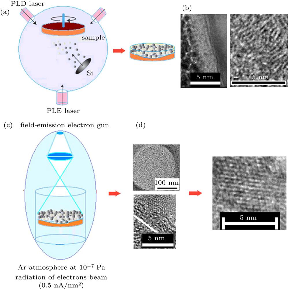
    Fig. 1. (a) Fabrication process of amorphous silicon nanofilm by using PLD method, (b) TEM images with nanofilm structure of amorphous silicon, (c) preparing process of silicene crystal by using coherent electron beam to irradiate amorphous silicon nanofilm, and (d) TEM image of spot shape occurring with coherent electron beam irradiating surface (left), and TEM image of the silicene crystal (right).
    (a) TEM image of silicene with hexagonal lattices, (b) TEM image of new silicene with rectangular lattices, with inset exhibiting electronic diffraction pattern of rectangular lattice.
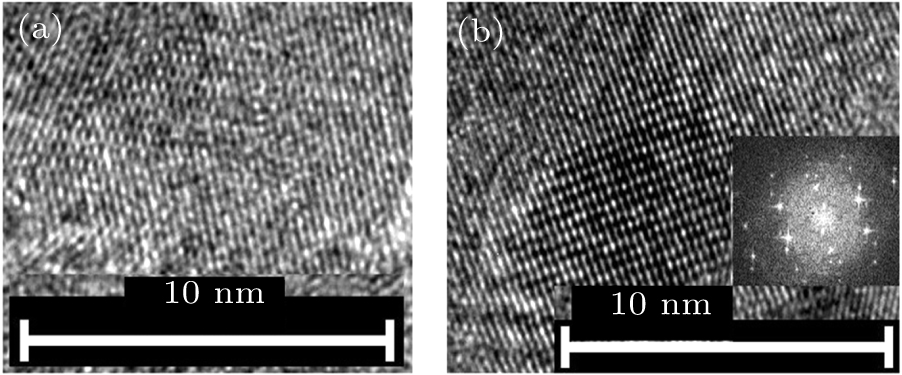
    Fig. 2. (a) TEM image of silicene with hexagonal lattices, (b) TEM image of new silicene with rectangular lattices, with inset exhibiting electronic diffraction pattern of rectangular lattice.
    Simulation model of ideal primal 2D silicon with hexagonal lattice passivated by hydrogen atoms (white balls), showing (a) laterally cross-cut structure of ideal primal model in 2D structure with hexagonal lattice, (b) overlook structure of ideal primal model in 2D structure with hexagonal lattice, (c) silicene structure with hexagonal lattice after optimizing process in simulating calculation, in which convex bond angle of silicon atom is about 115°, and (d) TEM image of silicene crystal with hexagonal lattice observed in experiment.
    Fig. 3. Simulation model of ideal primal 2D silicon with hexagonal lattice passivated by hydrogen atoms (white balls), showing (a) laterally cross-cut structure of ideal primal model in 2D structure with hexagonal lattice, (b) overlook structure of ideal primal model in 2D structure with hexagonal lattice, (c) silicene structure with hexagonal lattice after optimizing process in simulating calculation, in which convex bond angle of silicon atom is about 115°, and (d) TEM image of silicene crystal with hexagonal lattice observed in experiment.
    (a) Energy band structure calculated in simulation model of silicene with hexagonal lattice, where it has a direct bandgap of 1.4 eV and a nearly Dirac-cone-like shape at Γ point, (b) density distribution of states with localized peak near conduction band valley calculated in simulation model of silicene with hexagonal lattice.
    Fig. 4. (a) Energy band structure calculated in simulation model of silicene with hexagonal lattice, where it has a direct bandgap of 1.4 eV and a nearly Dirac-cone-like shape at Γ point, (b) density distribution of states with localized peak near conduction band valley calculated in simulation model of silicene with hexagonal lattice.
    Simulation model of 2D crystal with rectangular lattice, showing (a) laterally cross-cut structure of ideal primal model of 2D structure of silicon crystal with rectangular lattice, and (b) overlook structure of ideal primal model of 2D structure of silicon crystal with rectangular lattice.
    Fig. 5. Simulation model of 2D crystal with rectangular lattice, showing (a) laterally cross-cut structure of ideal primal model of 2D structure of silicon crystal with rectangular lattice, and (b) overlook structure of ideal primal model of 2D structure of silicon crystal with rectangular lattice.
    Change process in CASTEP geometry optimization of new silicene crystal with rectangular lattice, showing (a) change process of structure energy in optimization process, (b) new silicene crystal with rectangular lattice after optimizing process in simulating calculation, in which convex bond angle of silicon atom is about 118°, and (c) TEM image of new silicene crystal with rectangular lattice observed in experiment.
    Fig. 6. Change process in CASTEP geometry optimization of new silicene crystal with rectangular lattice, showing (a) change process of structure energy in optimization process, (b) new silicene crystal with rectangular lattice after optimizing process in simulating calculation, in which convex bond angle of silicon atom is about 118°, and (c) TEM image of new silicene crystal with rectangular lattice observed in experiment.
    (a) Calculated energy band structure for new silicene crystal with rectangular lattice showing a real direct bandgap of 0.78 eV and a nearly Dirac-cone-like shape in X region, and (b) simulated density distribution of states for new silicene crystal with rectangular lattice, showing localized peaks in bandgap.
    Fig. 7. (a) Calculated energy band structure for new silicene crystal with rectangular lattice showing a real direct bandgap of 0.78 eV and a nearly Dirac-cone-like shape in X region, and (b) simulated density distribution of states for new silicene crystal with rectangular lattice, showing localized peaks in bandgap.
    Wei-Qi Huang, Shi-Rong Liu, Hong-Yan Peng, Xin Li, Zhong-Mei Huang. Synthesis of new silicene structure and its energy band properties[J]. Chinese Physics B, 2020, 29(8):
    Download Citation