Visible light communication (VLC) technology is crucial in high-speed positioning, sensing, internet of things (IoT), and other fields because of its characteristics of high transmission rate, no band limit, safety, and eco-friendliness. With the development of VLC technology, indoor VLC technology has also received increased attention. The LED array is used as the transmitting unit in an indoor VLC system. However, the layout and parameters of a LED array affect the received illumination and optical power, thus changing the communication quality of receiving plane and affecting the fairness of user communication. Therefore, to solve the problem of uneven communication performance caused by conventional array layout, we propose a partial-nonuniform symmetrical layout by using a modified genetic algorithm. Considering the primary reflection of the wall, the number of light beads on the chips, the half power angles, and array layouts that can further improve the received optical power uniformity are designed to synchronously optimize the position of LED chips.
In this study, by studying and summarizing the common LED array layouts used in indoor VLC systems worldwide, a partial-nonuniform symmetrical array layout scheme was developed. The scheme was used to optimize the position of LED chips, number of light beads on the chip, and half power angles of the partial array. Thus, the entire surface of emission was obtained by folding the optimized nonuniform part before the optical power uniformity of the receiving surface was calculated based on the optimized array layout scheme. Thereafter, the VLC model with either non-line of sight link (NLOS) or line of sight (LOS) link was constructed. In addition, the crossover and variation operators in a genetic algorithm (GA) were modified via combination with the simulated annealing algorithm and self-adaption. Based on the LOS link and NLOS link models, an objective function that can synchronously optimize the position of LED chips, the number of light beads on the chip, and the half power angles was constructed. Finally, using the room model as the research object, the array layout was optimized by a modified genetic algorithm. Different side lengths of the room model, with a step length of 0.5 m, were considered. The LED array layouts in the room models of sizes 3 m×3 m×3 m, 5 m×5 m×5 m, and 7 m×7 m×7 m were examined, and the according parameters were determined; this demonstrated the versatility of the proposed scheme.
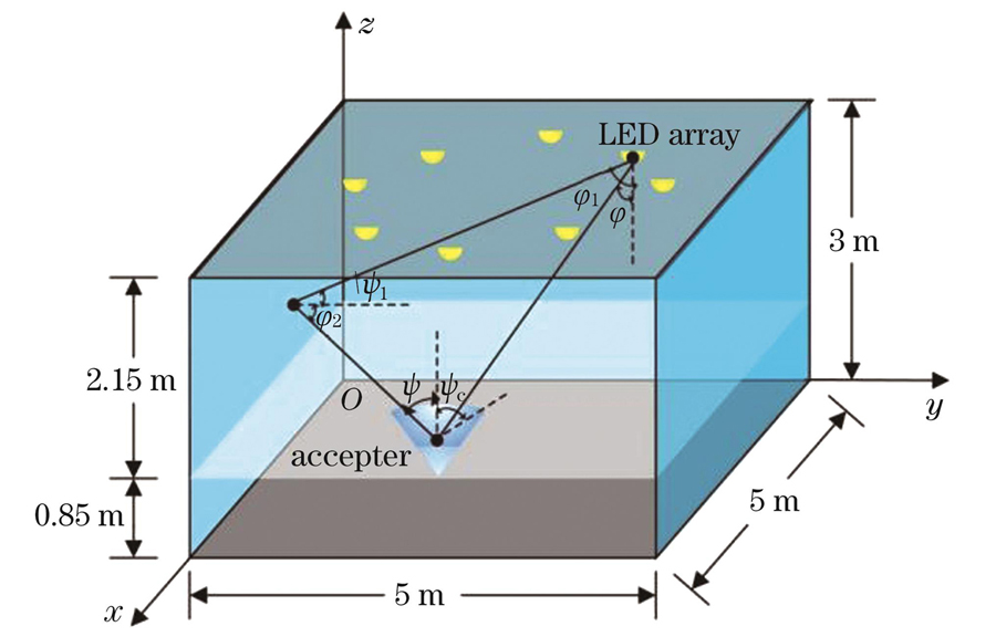
The proposed scheme was used to optimize the LED array. In the room model of size 5 m×5 m×3 m, considering the primary reflection, the optimized LED array layout (Fig. 3) was obtained. The position of LED chips, number of light beads on the chip, and half power angles of the LED chip are shown in Table 3. The received optical power uniformity reaches 97.7%, the maximum received illuminance is 1341 lx, the minimum received illuminance is 1089.9 lx, and the illumination uniformity is 0.84 [Fig.4 (a)]. The illuminance conforms to the specified international standardization range (300-1500 lx). The maximum received optical power is 1062 μw, and the minimum received optical power is 876.6 μw [Fig. 4 (b)], thus ensuring a high received optical power of the communication system. In the room models of sizes 3 m×3 m×3 m and 7 m×7 m×3 m, the optimized LED array layouts (Fig. 6) have four different LED chips. Their parameters are listed in Tables 4 and 5. In the 3 m×3 m×3 m room model, the illumination uniformity of is 0.88 [Fig.7 (a)] and the received optical power uniformity is 97.22% [Fig.7 (b)]. In the room model of size 7 m×7 m×3 m, the received illumination uniformity of is 0.9 [Fig.7 (c)], and the received optical power uniformity is 95.54% [Fig.7 (d)]. The received illuminance values of the two aforementioned layouts also meet the lighting standards. Moreover, the received optical power and illumination uniformity after the optimization of the room model were noted with a step length of 0.5 m (Fig.8). The results indicate that even if the room size varies, the received optical power uniformity maintains more than 95%, and the received illumination uniformity is always greater than 0.7, indicating that the proposed optimization method has strong versatility.