
Gui Cen, Zhi-Bin Zhang, Xin-Yu Lü, Kai-Hui Liu, Zhi-Qiang Li. Near-field infrared microscopy of graphene on metal substrate [J]. Acta Physica Sinica, 2020, 69(2): 027803-1
- Acta Physica Sinica
- Vol. 69, Issue 2, 027803-1 (2020)
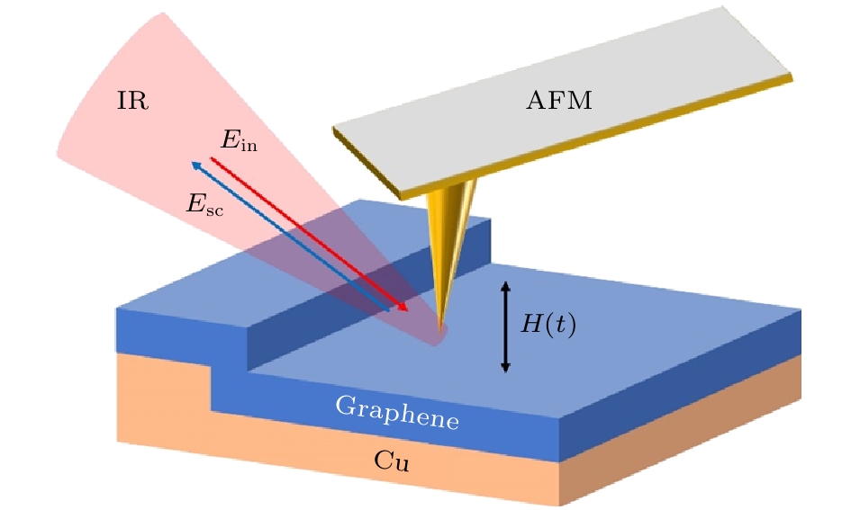
Fig. 1. Schematic of s-SNOM. An infrared light is focused between the sample and the probe tip, which oscillate vertically with frequency
and amplitude A . The tip-sample distance is
, where
is the minimum tip-sample distance. Incident light
interacts with tip-sample system, and is elastically scattered. The scattered field
encodes the properties of the sample surface.
s-SNOM示意图 一束红外光(IR)聚焦于针尖和样品之间, 针尖以频率
和振幅A 在竖直方向振动, 针尖与样品的距离为
, 其中
表示针尖和样品的最小距离, 测量信号是针尖-样品系统的散射光
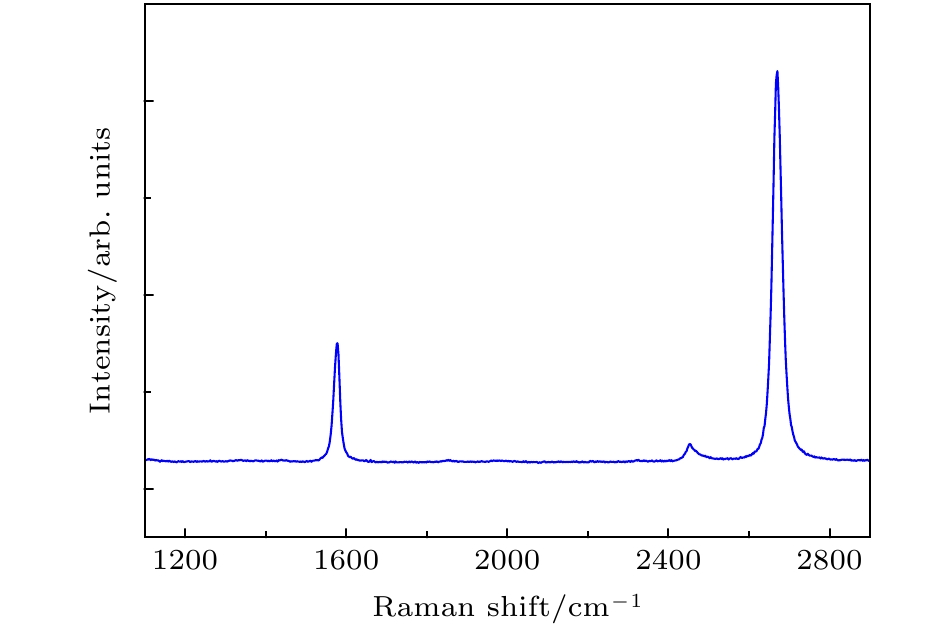
Fig. 2. Raman spectra of graphene on Cu substrate. The Lorentzian shape of 2D peak manifested that it is a monolayer graphene. Absence of D peak indicated its defect-free and high-quality nature.生长在铜衬底上的石墨烯拉曼光谱2D峰呈现了单个的洛伦兹峰型, 表明是单层石墨烯; D峰没有出现, 表明是无缺陷的高质量石墨烯
Fig. 3. s-SNOM images of a h-BN/Cu step: (a) Different tip positions when the tip is scanned across a step. ① and ④ are the tip positions far away from the step, ② and ③ are the positions where a peak (corresponding to the formation of two hot-spots) and a dip appear in the s-SNOM signal, respectively. The tip and the step are shown in proportion. Red circle drew on the tip represents its apex with diameter of D = 25 nm; (b) Zoom-in on the gap between tip and sample at tip position ② in (a), which shows the two hot-spots by red arrows; (c) left panel: topography (upper) and s-SNOM image (lower) of h-BN/Cu at a surface step. Right panel: topography (upper) and s-SNOM line-profiles (lower) corresponding to the blue solid lines in the left panel. Labels ①–④ are corresponding to those in (a). Black and red dash lines indicate different features (peak, dip and plateau) in the s-SNOM line-profile.
h-BN/Cu台阶成像图 (a) 针尖扫过台阶时的不同位置, ①和④表示针尖处于远离台阶的位置, ②和③分别表示信号峰值(两个热点形成处)和信号谷值对应的针尖位置, 图中的针尖与台阶以等比例画出, 针尖中的红色圆圈表示直径D = 25 nm的针尖尖端; (b) (a)中位置②处针尖与台阶边缘间隔的局部放大图, 红色箭头指出热点形成的位置; (c) 左侧: h-BN/Cu台阶的形貌(上)和s-SNOM成像(下); 右侧: 左侧图中蓝色实线对应的形貌(上)和s-SNOM信号(下), 其中标签①—④与(a)中的标签相对应, 黑色和红色虚线分别指出s-SNOM信号的不同特征(峰值、谷值和平台)
Fig. 4. s-SNOM images of two graphene/Cu samples with similar surface step geometries. In both cases, left panel: topography (upper) and s-SNOM image (lower); right panel: line-profiles of topography (upper) and s-SNOM line-profiles (lower) corresponding to the blue solid lines in left panel. (a) Case 1 (peak-dip): step height of about 5.3 nm and width of about 50 nm. Signal peak and dip appear corresponding to the lower and upper edge of the step, respectively; (b) Case 2 (peak): step height of about 5.5 nm and width of about 55 nm. Only a signal peak appears corresponding to the lower edge of the step.衬底台阶几何相近的两个石墨烯/铜样品的s-SNOM成像. 两种情况中, 左侧: 形貌(上)和s-SNOM成像(下); 右侧: 左侧图中蓝色实线对应的形貌(上)和s-SNOM信号(下) (a) 情况一, 台阶高度和宽度分别约为 5.3 nm和50 nm, 峰值和谷值分别对应台阶下方和下方边缘; (b)情况二, 台阶高度和宽度分别约为 5.5 nm和55 nm, 仅出现一个对应于台阶下方边缘的峰值


Set citation alerts for the article
Please enter your email address

© Copyright 2018-2021 | Chinese Laser Press. All Rights Reserved 沪ICP备15018463号-20