• Chinese Optics Letters
  • Vol. 17, Issue 7, 072501 (2019)
Yanhong Dong1, Qing Yang2, Guangqing Du1、*, Feng Chen1、**, Noor Uddin1, Dayantha Lankanath1, and Xun Hou1
Author Affiliations
  • 1State Key Laboratory for Manufacturing System Engineering and Key Laboratory of Photonics Technology for Information of Shaanxi Province, School of Electronics & Information Engineering, Xi’an Jiaotong University, Xi’an 710049, China
  • 2School of Mechanical Engineering, Xi’an Jiaotong University, Xi’an 710049, China
  • show less
    DOI: 10.3788/COL201917.072501 Cite this Article Set citation alerts
    Yanhong Dong, Qing Yang, Guangqing Du, Feng Chen, Noor Uddin, Dayantha Lankanath, Xun Hou. Electronic manipulation of near-field nanofocusing in few-layer graphene-based hybrid nanotips[J]. Chinese Optics Letters, 2019, 17(7): 072501 Copy Citation Text show less
    Schematic of the simulated FLG-based nanotip hybrid system. The graphene-coated Au tip is modeled as a conical taper terminated by a hemisphere of radius R as its point and elevated a distance d above a SiO2–graphene–SiO2 substrate. An electromagnetic plane wave is incident at an angle θ with respect to the surface normal. A 300-nm-thick perfectly matched layer (PML) encloses the simulation domain.
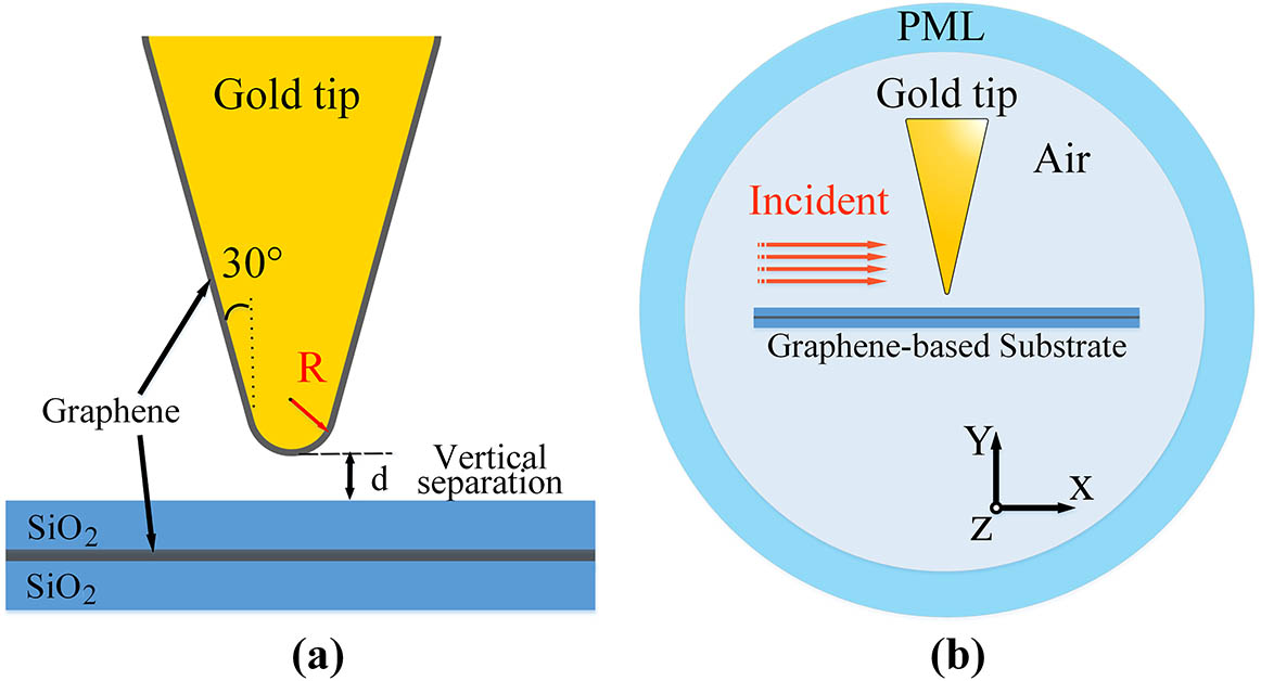
    Fig. 1. Schematic of the simulated FLG-based nanotip hybrid system. The graphene-coated Au tip is modeled as a conical taper terminated by a hemisphere of radius R as its point and elevated a distance d above a SiO2–graphene–SiO2 substrate. An electromagnetic plane wave is incident at an angle θ with respect to the surface normal. A 300-nm-thick perfectly matched layer (PML) encloses the simulation domain.
    Cross-section of mono-graphene-based nanotip structure. Calculated images of the e-field distributions in the case of mono-graphene in the substrate (The curvature radius of the nanotip is R=30 nm. The vertical spacing between the nanotip and substrate is d=20 nm, and incident light travels along the X direction).
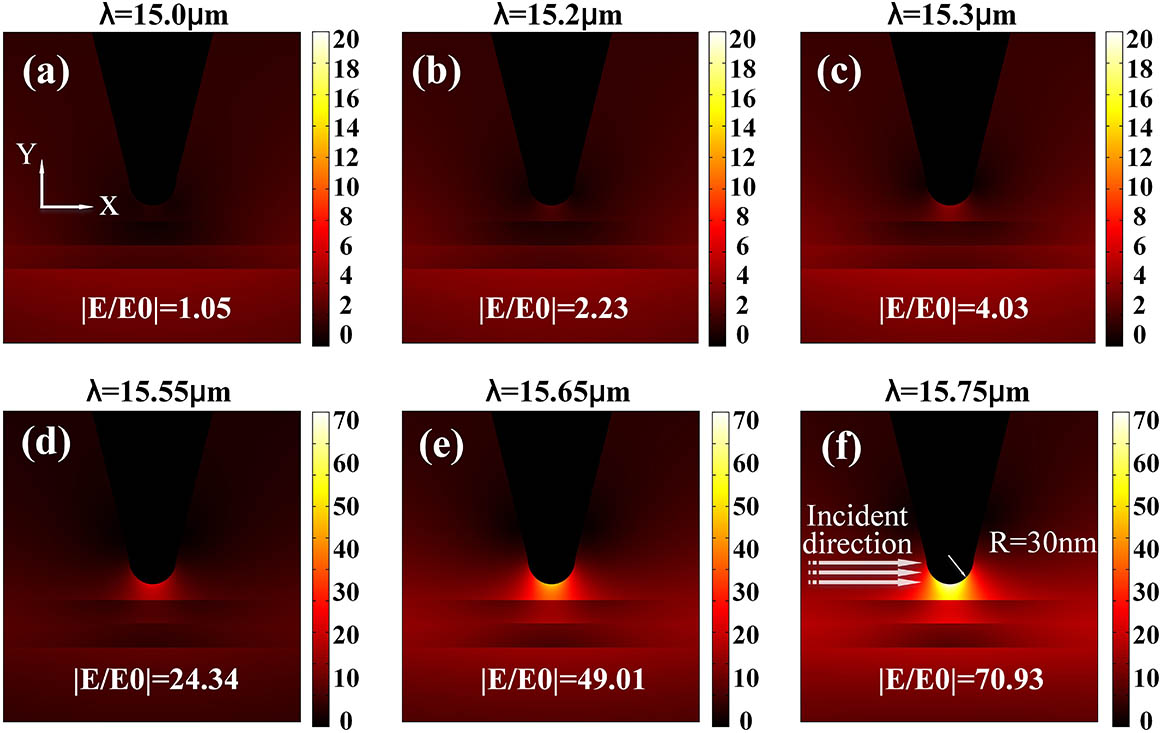
    Fig. 2. Cross-section of mono-graphene-based nanotip structure. Calculated images of the e-field distributions in the case of mono-graphene in the substrate (The curvature radius of the nanotip is R=30nm. The vertical spacing between the nanotip and substrate is d=20nm, and incident light travels along the X direction).
    Permittivity of MLG with respect to different Fermi energies. (a) The red, blue, black, green, and orange lines are corresponding to 0.1, 0.2, 0.3, 0.4, and 0.5 eV, respectively. (b) The normalized e-field enhancement and resonant frequency of the nanotip hybrid system depending on the Fermi energy of excited graphene. (c) Real and (d) imaginary parts of graphene permittivity with respect to the layers of FLG changing from 1 to 5 (EF is biased to 0.5 eV).
    Fig. 3. Permittivity of MLG with respect to different Fermi energies. (a) The red, blue, black, green, and orange lines are corresponding to 0.1, 0.2, 0.3, 0.4, and 0.5 eV, respectively. (b) The normalized e-field enhancement and resonant frequency of the nanotip hybrid system depending on the Fermi energy of excited graphene. (c) Real and (d) imaginary parts of graphene permittivity with respect to the layers of FLG changing from 1 to 5 (EF is biased to 0.5 eV).
    Simulation results of the electronic manipulation of near-field nanofocusing in a five-layer FLG-based tip structure. (a) The normalized e-field enhancement spectra with respect to different Fermi energies (The Fermi energy decreases with 0.1 eV step size from left to right). (b) The Fermi energy of FLG (black line) and the resonant wavelength (red line) are plotted as a function of the carrier concentration of FLG. The inset illustrates the calculated image of the localized e-field.
    Fig. 4. Simulation results of the electronic manipulation of near-field nanofocusing in a five-layer FLG-based tip structure. (a) The normalized e-field enhancement spectra with respect to different Fermi energies (The Fermi energy decreases with 0.1 eV step size from left to right). (b) The Fermi energy of FLG (black line) and the resonant wavelength (red line) are plotted as a function of the carrier concentration of FLG. The inset illustrates the calculated image of the localized e-field.
    Yanhong Dong, Qing Yang, Guangqing Du, Feng Chen, Noor Uddin, Dayantha Lankanath, Xun Hou. Electronic manipulation of near-field nanofocusing in few-layer graphene-based hybrid nanotips[J]. Chinese Optics Letters, 2019, 17(7): 072501
    Download Citation