• Acta Physica Sinica
  • Vol. 68, Issue 18, 187102-1 (2019)
Tian-Hui Wang1, Ang Li1, and Bai Han2、*
Author Affiliations
  • 1School of Disciplinary Basics and Applied Statistics, Zhuhai College of Jilin University, Zhuhai 519041, China
  • 2Key Laboratory of Engineering Dielectrics and Its Application, Ministry of Education, Heilongjiang Provincial Key Laboratory of Dielectric Engineering, School of Electrical and Electronic Engineering, Harbin University of Science and Technology, Harbin 150080, China
  • show less
    DOI: 10.7498/aps.68.20190859 Cite this Article
    Tian-Hui Wang, Ang Li, Bai Han. First-principles study of graphyne/graphene heterostructure resonant tunneling nano-transistors[J]. Acta Physica Sinica, 2019, 68(18): 187102-1 Copy Citation Text show less
    Schematic bipolar device models constructed with the SGDY (above panel) or NGDY (below panel) as center scattering region and the graphene nanoribbons as semi-infinite electrodes (source and drain in pink areas). The apex and edge carbon atoms are passivated by hydrogen atoms, and black frames indicate periodic unit cells.SGDY (上图)和NGDY (下图)纳米带两端连接石墨烯纳米带半无限电极(源极和漏极粉色区域)构建的双极器件模型, 石墨炔尖端和石墨烯边缘碳原子由氢原子钝化, 黑色框架表示周期性单胞
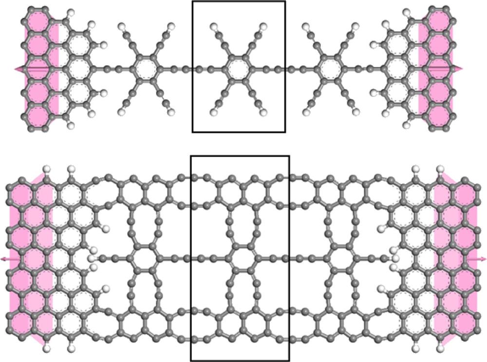
    Fig. 1. Schematic bipolar device models constructed with the SGDY (above panel) or NGDY (below panel) as center scattering region and the graphene nanoribbons as semi-infinite electrodes (source and drain in pink areas). The apex and edge carbon atoms are passivated by hydrogen atoms, and black frames indicate periodic unit cells.SGDY (上图)和NGDY (下图)纳米带两端连接石墨烯纳米带半无限电极(源极和漏极粉色区域)构建的双极器件模型, 石墨炔尖端和石墨烯边缘碳原子由氢原子钝化, 黑色框架表示周期性单胞
    Electronic energy band structure of SGDY (a) and NGDY (b) nanoribbons with Fermi energy level as reference energy zero (horizontal dashed line).SGDY (a)和NGDY (b)纳米带的电子能带结构, 以费米能级(水平虚线)为能量参考零点
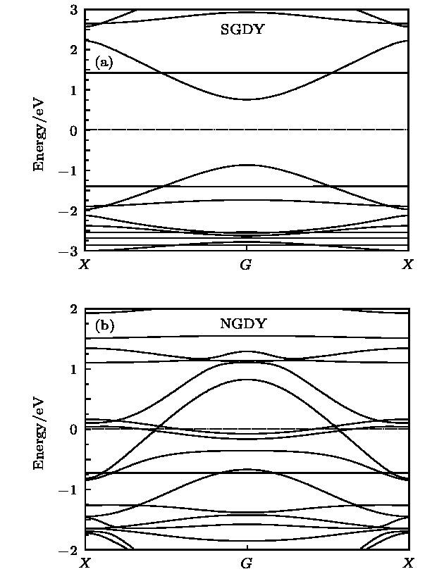
    Fig. 2. Electronic energy band structure of SGDY (a) and NGDY (b) nanoribbons with Fermi energy level as reference energy zero (horizontal dashed line).SGDY (a)和NGDY (b)纳米带的电子能带结构, 以费米能级(水平虚线)为能量参考零点
    Electron transport calculation in transistor model of bipolar devices with the SGDY/graphene nanoribbons heterostructure as the center scattering region and semi-infinite electrodes (source and drain) respectively under the gate voltage in vertical direction. The pink areas indicate electrodes, and the gray, white, red, yellow and pink spheres represent carbon, hydrogen, oxygen, silicon and aluminium atoms respectively.在SGDY/石墨烯异质结纳米带双极器件的垂直方向施加栅极电压构建的晶体管电子输运计算模型, 粉色区域表示电极, 灰色、白色、红色、黄色和粉色小球分别代表碳、氢、氧、硅和铝原子
    Fig. 3. Electron transport calculation in transistor model of bipolar devices with the SGDY/graphene nanoribbons heterostructure as the center scattering region and semi-infinite electrodes (source and drain) respectively under the gate voltage in vertical direction. The pink areas indicate electrodes, and the gray, white, red, yellow and pink spheres represent carbon, hydrogen, oxygen, silicon and aluminium atoms respectively.在SGDY/石墨烯异质结纳米带双极器件的垂直方向施加栅极电压构建的晶体管电子输运计算模型, 粉色区域表示电极, 灰色、白色、红色、黄色和粉色小球分别代表碳、氢、氧、硅和铝原子
    Drain current of SGDY and NGDY nanoribbon transistors varying with bias voltage under (a) Ug = 0 V and (b) Ug = 4 VSGDY和NGDY纳米带晶体管的漏极电流随偏置电压的变化 (a) Ug = 0 V; (b) Ug = 4 V
    Fig. 4. Drain current of SGDY and NGDY nanoribbon transistors varying with bias voltage under (a) Ug = 0 V and (b) Ug = 4 V SGDY和NGDY纳米带晶体管的漏极电流随偏置电压的变化 (a) Ug = 0 V; (b) Ug = 4 V
    Electron transmission spectra of SGDY nanoribbon transistors in the bias voltage range of 0−1.0 V under gate voltageUg = 4 V.SGDY纳米带晶体管在偏置电压0—1.0 V范围内的电子透射谱(栅极电压Ug = 4 V)
    Fig. 5. Electron transmission spectra of SGDY nanoribbon transistors in the bias voltage range of 0−1.0 V under gate voltageUg = 4 V. SGDY纳米带晶体管在偏置电压0—1.0 V范围内的电子透射谱(栅极电压Ug = 4 V)
    电子态描述及求解方法计算方案参数设置
    交换相关泛函GGAPBEsol[24]
    电子与原子实相互作用(core treatment)全电子相对论(all electron relativistic)
    数值基组双数值极化(DNP)
    轨道截至(orbital cutoff)Global5.0 Å
    SCF容忍度1 × 10⁻⁶ Ha/原子 (1 Ha = 27.2 eV)
    多极展开八极
    密度混合电荷和自旋混合幅度分别为0.2和0.5
    轨道占据热拖尾(smearing)[25]0.001 Ha
    布里渊区积分k点取样(电子结构) Monkhorst-Pack格点[26]1 × 1 × 25
    计算范德瓦耳斯相互作用DFT交换-相关泛函色散校正[27]
    布里渊区积分k点取样(电子输运) 均匀间隔格点间隔0.02/Å
    泊松求解法和泊松边界条件(电子输运)器件侧面缓冲长度7.5 Å
    泊松网格最大格点间距0.5 Å
    电极界面边界条件Dirichlet
    非电极界面边界条件Neumann
    电极边界区缓冲长度3 Å
    Table 1. Scheme and parameter setting up in calculationswith Dmol3 program.
    纳米带散射区电极研究方法栅极电压 /VPVR数据来源
    SGDY, NGDY石墨烯第一原理计算54.5, 6.0本文
    BN石墨烯理论计算和实验0, 201—4Ref. [16]
    BN石墨烯理论计算和实验–40, 0, 40Ref. [17]
    GaN-Al-GaNGaN理论计算(Matlab)–1, –2, –32.66Ref. [19]
    Table 2. PVR for nanoribbon transistors fabricated with different materials under different gate voltage.
    Tian-Hui Wang, Ang Li, Bai Han. First-principles study of graphyne/graphene heterostructure resonant tunneling nano-transistors[J]. Acta Physica Sinica, 2019, 68(18): 187102-1
    Download Citation