Abstract
Metal hydrazone complex thin films are used as laser patterning materials, and the patterns with a minimum resolution of about 78 nm are successfully obtained by the laser writing setup (, ). The minimum resolution is only about 1/8 of the writing spot size. In the formation of patterns, there is only a single step for forming patterns by the laser heating-induced clear thermal gasification threshold effect without any other development processes such as wet etching. This work provides an effective method for directly achieving nanoscale-resolved pattern structures with diode-based maskless laser writing lithography at visible light wavelengths.Semiconductor diode-based maskless laser direct writing is a good method for pattern fabrication because of its many advantages over other methods, such as large area patterning, operation in the far-field range and in air, low fabrication cost, controllability, and arbitrary structure fabrication[1]. However, there are fatal disadvantages: the pattern resolution is very difficult to reduce down to the nanoscale due to the optical diffraction limit[2]. Although femtosecond-based laser fabrication and two-beam lithography are feasible methods for nanoscale patterning[3–9], the fabrication cost is high, and the speed is slow. Therefore, new techniques are needed to enable the fast and cheap realization of the large-area high-speed fabrication of nanoscale-resolved arbitrary pattern structures.
In nanoscale-resolved maskless laser direct writing, nonlinearity-induced super-resolution lithography is a good way to obtain a subwavelength pattern resolution[10–15]. Another alternative method is laser thermal lithography, which uses a single light beam with several milliwatts of power from a laser diode. The laser thermal lithography material absorbs the laser energy and is heated to a certain temperature, such as a phase change or melting point, to form various patterns on the material’s surface. In laser thermal lithography, the thermal change of the material occurs over the whole area inside the laser beam spot, and the pattern, whose size is almost determined by the writing laser beam’s spot size, is formed[16–18]. However, for heat-mode laser writing lithography, which is based on the manufacturing technique for optical discs, the thermally induced structural change of the material occurs only at the center of the laser beam spot because of the threshold effect[19]. A pattern whose size is smaller than the spot size can be formed. Generally, the laser thermal lithography materials are from inorganic chalcogenide phase change thin films due to selective wet etching between the crystalline and amorphous phases[20–25]. In this work, we give a single-step method to directly form nanoscale-resolved patterns by heat-mode maskless direct laser writing lithography on metal hydrazone complex (MHC) thin films due to the clear gasification threshold effect[26]. This is compared with inorganic material-based laser thermal lithography, no other developing processes such as wet-etching are required[27], and the MHC thin films can be directly gasified under the writing laser beam heat without experiencing a phase change process, such as crystallization and melting. The writing power is only several milliwatts, and the nanoscale-resolved patterns can be directly formed by the clear gasification threshold effect.
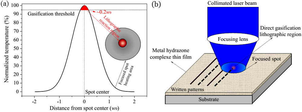
According to the characteristics of the gasification threshold effect, the lithographic reaction localized at a very small region can be schematically illustrated as follows. As shown in Fig. 1, a focused spot with a Gaussian intensity profile irradiates onto the MHC thin films. The spot intensity profile can be expressed as , where is a radial coordinate and is the spot radius at intensity. For laser writing lithography, the lithographic reaction originates from the light energy absorption. The light energy absorption can be estimated as , where is the absorption coefficient. The MHC thin films are quickly heated by the irradiation of the writing laser beam.
Sign up for Chinese Optics Letters TOC. Get the latest issue of Chinese Optics Letters delivered right to you!Sign up now

Figure 1.Formation of localized lithographic region. (a) Temperature rise profile and localization lithographic region induced by the gasfication threshold effect. (b) The schematic of directly writing nanoscale-resolved patterns on MHC thin films.
By neglecting the heat diffusion and loss, the normalized profile of the temperature rise can be also considered to be a Gaussian profile, as shown in Fig. 1(a). For the MHC thin films, the gasification shows a very clear threshold effect. One can make full use of the clear gasification threshold effect and reduce the lithographic region. As an example, one can assume that the threshold temperature is at 95% of the maximum temperature rise; thus, the lithographic reaction takes place in only in a very small area with a diameter of about as shown in the inset of the Fig. 1(a). When compared with the focused spot itself, the pattern resolution is greatly reduced to below the diffraction limit through the gasfication threshold effect. The nanoscale-resolved patterns can be directly written in the MHC thin films by sample stage movements or by laser writing scanning the sample, as shown in Fig. 1(b).
In order to satisfy the requirements of nanoscale-resolved direct patterning using several milliwatts of laser power, the designed materials are required to have the following basic features: (1) proper absorption at the writing laser wavelength, (2) the lithographic reaction taking place at a laser power of a milliwatt magnitude, (3) localizing the lithographic region to the subwavelength scale or even the nanoscale, and (4) direct patterning without wet-etching and developing processes.
In this work, based on the requirements for nanoscale-resolved direct-patterning materials, we choose MHC thin films as the laser thermal lithography materials. The MHC materials are provided by our laboratory. The thermal gravimetric (TG) and differential thermal (DSC) analyses are shown in Fig. 2. The TG analysis was measured using an STA 449F3 (Netzsch, Germany) at a heating rate of 10°C/min under protection, and Fig. 2(a) presents the experimental results. One can see that the weight abruptly decreases to 70% at about 300°C, which indicates that the MHC thin films are partially gasified at 300°C. The gasification shows a clear threshold effect. The gasification threshold is marked as . The gasification presents an exothermal reaction, and the temperature range is less than 10°C, which can be seen from the DSC analysis shown in Fig. 2(b). Therefore, the lithographic patterns can be directly formed at a laser power of a milliwatt magnitude on the MHC thin films directly because of the abruptly weight loss in a short temperature range, which is the advantage of the MHC thin film as a laser thermal lithography material. There is only a single-step process for the pattern formation, without any other developing processes such as wet etching required in the process of the formation of lithographic patterns.
Figure 2.Thermal properties of MHC. (a) TG and (b) DSC.
The thin films were prepared by dissolving MHC materials in acetone and propylene glycol methyl ether acetate at concentrations of 3–10 wt. %. They were spin coated onto glass substrates at a spin speed of 800–1500 rpm. The surface morphology of the prepared thin films was obtained through atomic force microscopy (AFM), and is shown in Fig. 3(a). One can see that the root mean square of the surface roughness is less than 0.5 nm, which indicates that the surface of thin films is very homogeneous and smooth. The absorption spectrum is presented in Fig. 3(b). The absorption peak is at about the 456 nm wavelength, and the band tail occurs at about the 550 nm wavelength. There is strong absorption at a laser wavelength of 405 nm, and the corresponding absorption intensity is 0.68. This is a large value and guarantees the lithographic reaction is taking place at a laser power of a milliwatt magnitude.
Figure 3.(a) Surface morphology and (b) absorption light spectrum at a visible light wavelength of the prepared thin films.
The direct laser writing was conducted using a diode-based direct laser writing setup at a visible light wavelength. A semiconductor GaN diode laser device with a wavelength of 405 nm was used as the writing light source. Here, it is explained that GaN diode lasers have been applied in many fields, including surface plasmon-enhanced micro-cylinder modes in photonic quasi-crystals[28], due to their advantages of a short wavelength, compactness, and good stability. An objective lens with an NA of 0.90 was used to focus the writing light beam onto a diffraction-limited spot. The writing spot size is theoretically . However, the spot is actually about 600 nm, which is slightly larger than the diffraction-limited spot size because the setup is not perfect in our experiment. The patterns can be written in different modes, but in this work, the patterns are written in the pulsed light mode. There are two ways to use the sample stage movement: the grating-scan way, and the vector-scan way. In our experiments, the grating-scan way is used, and the sample structure is designed as a “glass substrate (1.2 mm)/MHC thin film (100 nm)”. The laser beam is directly focused onto the surface of the MHC thin films. The laser power and pulse width can be arbitrarily tuned according to the experimental requirements, and a detailed description of experimental setup can be found[29].
Figure 4 gives the typical experimental results of pit-shaped patterns. Figure 4(a) is the pit-shaped patterns written at laser power of and pulse width of , the pit diameter is about 196 nm, which is about 1/3 the writing spot size [as shown in Fig. 4(a-a1)]. The depth is 10 nm, which can be seen from the Fig. 4(a-a2). Figure 4(a-a3) is the three-dimensional image of the Fig. 4(a-a1), where the uniform pits are directly written on the MHC thin films. The pit size depends greatly on the laser power and pulse width. The very small pits are obtained by optimizing the laser power and pulse width. The optimum experimental results are given in Fig. 4(b), where the laser power and pulse width are 2 mW and 20 ns, respectively. Figure 4(b-b1) is the two-dimensional image and Fig. 4(b-b2) is the cross-section profile of a single pit. The pit size is about 98 nm, which is only about 1/6 the writing spot size. Figure 4(b-b3) is the three-dimensional image of Fig. 4(b-b1), and the small pit patterns are uniform.
Figure 4.AFM images of the patterns directly written on the MHC thin film. (a) Pit-shaped patterns written at and : (a1) two-dimensional image, (a2) cross-sectional profile, and (a3) three-dimensional image; (b) pit-shaped patterns written at and : (b1) two-dimensional image, (b2) cross-sectional profile, and (b3) three-dimensional image; (c) line-shaped patterns written at and : (c1) two-dimensional image, (c2) cross-sectional profile, and (c3) three-dimensional image; (d) coarse line written at and : (d1) two-dimensional image, (d2) cross-sectional profile, and (d3) three-dimensional image.
The line-shaped patterns are also written on the MHC thin films using the pulse light mode. Figure 4(c) presents the experimental results obtained at and . Figure 4(c-c1) is the two-dimensional image, and the line width is 141 nm, which is about 1/4 the writing spot size. Figure 4(c-c2) is the cross-section profile along the marked line of Fig. 4(c-c1), where the depth of the line is about 8 nm. Figure 4(c-c3) is the three-dimensional image; one can see that the line-shaped patterns are very uniform and clear. By analyzing the Figs. 4(a) and 4(c), one can find that the pit/line depth of the patterns decreases when the pattern resolution increases, and the depth is not more than 10 nm. Actually, the depth can greatly increase through a high laser power or long pulse width. Figure 4(d) gives the coarse line obtained at and . The line width is 2.5 μm [shown in Fig. 4(d-d1)], and the depth is about 80 nm [shown in Fig. 4(d-d2)]. Figure 4(d-d3) is the three-dimensional image of Fig. 4(d-d1).
For laser thermal lithography, the pattern resolution is influenced by the in-plane and out-of-plane heat diffusion channels[30]. The in-plane heat diffusion channel tends to increase the pattern linewidth or pit size; however, the out-of-plane heat diffusion channel tends to decrease the pattern linewidth or pit size. In order to reduce negative influence of in-plane heat diffusion on the pattern resolution, the heat diffusion channel is manipulated by inserting a metal thin film between the substrate and MHC thin film, where the metal thin film functions as a thermal sink.
The sample structure is designed as a “glass substrate (1.2 mm)/metal layer (100 nm)/MHC thin films (100 nm),” where Ag is used as the metal layer and functions as thermal sink. The Ag thin film is deposited onto the glass substrate through the magnetron-controlled sputtering method. The MHC thin films are prepared on the Ag layer by the spin-coating method. In the process of writing, the laser beam is directly focused onto the MHC thin films. By inserting the thermal sink of the Ag thin film in between the substrate and the MHC thin film, the out-of-plane heat diffusion dominates over the in-plane heat diffusion; thus, the pattern resolution can be further improved.
Figure 5(a) gives the optimized experimental results, where the writing laser power and pulse width are 3 mW and 15 ns, respectively. Figures 5(a-a1) and 5(a3) are the two-dimensional and three-dimensional images of the written pit-shaped patterns, respectively. Figure 5(a-a2) is the cross-section profile along the marked line of Fig. 5(a-a1): the pit-shaped patterns are uniform and clear, and the size of every pit is about 78 nm, which is only about 1/8 the writing spot size. The pit depth is about 3 nm, which is small and needs to be improved in the next work. In order to compare the sample with the thermal sink of the Ag thin film, Fig. 5(b) presents the experimental results of the sample without the thermal sink of the Ag thin film, where the writing laser power and pulse width are the same as Fig. 5(a). Figures 5(b-b1) and 5(b-b3) are the two-dimensional and three-dimensional images of the written pit-shaped patterns, respectively. Figure 5(b-b2) is the cross-section profile along the marked line of Fig. 5(b-b1): the pit-shaped patterns are uniform and clear, and the size of every pit is about 118 nm, which is only about 1/5 the writing spot size. In a comparison of Fig. 5(a) with Fig. 5(b), one can see that the thermal sink of the Ag thin film is very useful for further improving the pattern resolution by manipulating the heat flow direction.
Figure 5.AFM images of the patterns written at and . (A) The sample with the thermal sink of the Ag thin film: (a1) two-dimensional image, (a2) cross-sectional profile, and (a3) three-dimensional image; (B) without thermal sink of Ag thin film: (b1) two-dimensional image, (b2) cross-sectional profile, and (b3) three-dimensional image.
From the above experimental results, one can see that with the decrease of the laser power and pulse width, the sizes of the patterns are reduced. Theoretically, based on Fig. 1(a), the thermal lithographic resolution can become infinitely small due to the Gaussian profile characteristics of the focused spot intensity. However, on one hand, there is the in-plane heat diffusion channel, which tends to increase the pattern linewidth; on the other hand, the pattern contrast is required. Thus, it is hard to further achieve the very small pattern feature size. In this work, the smallest feature size of the patterns is 78 nm. The feature size may be further reduced through using the combination of an optical nonlinear response and laser thermal lithography. Additionally, nanoscale-resolved structures with a shallow depth can be applied to the fabrication of a nanoimprint template or quantum dots, etc.
In addition, the pattern transfer is conducted, and the pattern transfer processes are as follows. First, the pit-shaped patterns are directly written on the surface of MHC thin film at the writing parameters of and . The written patterns are shown in Fig. 6(a), where the pit size is about 375 nm. Second, dry etching using ICP is carried out, where the etching gas is a mixture of and Ar, the ratio of to Ar is , and the pressure is 1 Pa. After dry etching, the MHC thin film is removed using acetone. The patterns transferred to the surface of the fused silica substrate are observed using scanning electronic microscopy, and Fig. 6(b) gives the results. One can see that the pit-shaped patterns are successfully transferred to the fused silica substrate, and the pit size is about 358 nm, which is close the size of the pits in Fig. 6(a). The physical mechanism of the pattern transfer and ICP etching processes need be further explored in future work.
Figure 6.Results of pattern transfer: (a) patterns on the MHC thin films obtained at and . (b) Patterns are transferred from MHC thin film to the fused silica substrate by ICP dry-etching method.
In conclusion, we use MHC thin films as laser thermal lithographic patterning materials; the nanoscale-resolved patterns are directly written on the MHC thin films. Using the laser writing setup with a GaN diode emitting 405 nm wavelength light as a laser source and an objective lens with an NA of 0.90 as the focusing lens, where the focusing spot size is actually about 600 nm, patterns with a minimum feature size of about 78 nm are successfully obtained, experimentally. The pattern size is only about 1/8 the writing spot size. In addition, the patterns are successfully transferred to the fused silica substrate using the ICP dry-etching method. Compared with the previous works, we obtained the large-area and high-speed fabrication of nanoscale-resolved patterns in air with only a single step, without any other developing processes such as wet etching required. This work provides a simple and effective method for directly forming nanoscale-resolved patterns.
References
[1] C. A. Rothenbach, M. C. Gupta. Opt. Laser Eng., 50, 900(2012).
[2] T. Grosjean, D. Coujon, C. Bainier. Opt. Lett., 32, 976(2007).
[3] Z. Gan, Y. Cao, Ri. A. Evans, M. Gu. Nat. Commun., 4, 2061(2013).
[4] L. Li, R. R. Gattass, E. Gershgoren, H. Hwang, J. T. Fourkas. Science, 324, 910(2009).
[5] J. W. Perry. Science, 324, 892(2009).
[6] T. L. Andrew, H. Tsai, R. Menon. Science, 324, 917(2009).
[7] T. Scott, B. Kowalski, A. Sullivan, C. Bowman, R. McLeod. Science, 324, 913(2009).
[8] Y. Cao, M. Gu. Appl. Phys. Lett., 103, 213104(2013).
[9] F. Meng, J. Hu, W. Han, P. Liu, Q. Wang. Chin. Opt. Lett., 13, 062201(2015).
[10] X. Zhang, J. Wei. Photon. Res., 3, 100(2015).
[11] J. Wei, J. Liu, X. Jiao. Appl. Phys. Lett., 95, 241105(2009).
[12] J. Wei, R. Wang. J. Appl. Phys., 115, 123102(2014).
[13] Y. Zha, J. Wei, F. Gan. Opt. Commun., 304, 49(2013).
[14] X. Ma, J. Wei. Nanoscale, 3, 1489(2011).
[15] J. Wei. Nonlinear Super-Resolution Nano-Optics and Applications(2015).
[16] J. Wei, Q. Liu, M. Xiao. Appl. Surf. Sci., 280, 89(2013).
[17] A. Dun, J. Wei, F. Gan. Thin Solid Films, 519, 3859(2011).
[18] A. Dun, J. Wei, F. Gan. Appl. Phys. A, 103, 139(2011).
[19] M. Kuwahara, J. H. Kim, J. Tominaga. Microelectron. Eng., 73, 69(2004).
[20] C. Deng, Y. Geng, Y. Wu, Y. Wang, J. Wei. Microelectron. Eng., 103, 7(2013).
[21] A. Dun, J. Wei, F. Gan. Chin. Opt. Lett., 9, 082101(2011).
[22] H. Li, Y. Geng, Y. Wu. Appl. Phys. A, 107, 221(2012).
[23] T. Shintani, Y. Anzai, H. Minemura, H. Miyamoto, J. Ushiyama. Appl. Phys. Lett., 85, 639(2004).
[24] H. Cheng, C. Jong, C. Lee, T. Chin. IEEE Trans. Magn., 41, 1031(2005).
[25] M. Kuwahara, J. Li, C. Mihalcea, N. Atoda, J. Tominaga, L. Shi. Jpn. J. Appl. Phys., 41, L1022(2002).
[26] C. Deng, Y. Geng, Y. Wu. J. Mater. Chem. C, 1, 2470(2013).
[27] J. Cheng, N. Yan. Chin. Opt. Lett., 13, 082201(2015).
[28] Z. Y. Fang, T. Dai, Q. Fu, B. Zhang, X. Zhu. J. Micro. (Oxford), 235, 138(2009).
[29] R. Wang, J. Wei, Y. Fan. Opt. Express, 22, 4973(2014).
[30] J. Wei, Y. Wang, Y. Wu. Opt. Express, 22, 32470(2014).