National Laboratory of Solid State Microstructures, Key Laboratory of Intelligent Optical Sensing and Manipulations, Jiangsu Key Laboratory of Artificial Functional Materials, College of Engineering and Applied Sciences, Nanjing University, Nanjing 210093, China
Zhizhang Wang, Wange Song, Yuxin Chen, Bin Fang, Jitao Ji, Haoran Xin, Shining Zhu, Tao Li, "Metasurface empowered lithium niobate optical phased array with an enlarged field of view," Photonics Res. 10, B23 (2022)
Copy Citation Text
Integrated optical phased arrays (OPAs) have attracted significant interest to steer laser beams for applications including free-space communications, holography, and light detection and ranging. Although many methods have been proposed to suppress grating lobes, OPAs have also been limited by the trade-off between field of view (FOV) and beamforming efficiency. Here, we propose a metasurface empowered port-selected OPA (POPA), an OPA steered by port selection, which is implemented by an aperiodic waveguide array with an average pitch less than the wavelength and phase controlled by coupling among waveguides. A metasurface layer above the POPA was designed to increase wide FOV steering, aliasing-free by polarization division. As a result, we experimentally demonstrate beam scanning over a FOV. The aliasing-free POPA with expanded FOV shows successful incorporation of the waveguide-based OPA technique with an emerging metasurface design, indicating much exploration in concepts for integrated photonic devices.
1. INTRODUCTION
Light detection and ranging (LIDAR) provides relatively long-range and high-precision 3D imaging, essential for future autonomous vehicles [1–4]. The optical phased array (OPA) is a key component of LIDAR, and OPAs have been recently proposed as a promising solid state technology to achieve full integration due to its low material cost, high integration, and compatibility with CMOS technology [5–9]. OPA has been explored on various photonic platforms, and silicon nitride () has recently become of interest for waveguides in integrated OPAs due to allowing for higher input power, larger transparency, and lower phase variation [10–14]. Compared with , lithium niobate (LN) has not only the same advantages as , but also excellent electro-optic (EO) Pockels material with a large coefficient [15–19]. With the development of thin-film LN technology, the LN-on-insulator (LNOI) platform shows great potential for OPAs.
The OPA technique keeps moving towards high performances, such as a wide field of view (FOV), aliasing-free, high scanning speed, low power consumption, and small size. Unlike radio frequency (RF) phased arrays, emitting antennas cannot be spaced by a half-wavelength, and uniformly spaced antenna arrays lead to typically unwanted grating lobes and sidelobes when the emitter spacing is larger than half-wavelength. Well-designed aperiodic arrays have been proposed as a promising approach to achieve a wide steering range and high resolution simultaneously at the cost of decreased main lobe efficiencies and signal-to-noise ratios (SNRs) [20–24]. Recently, a new beam steering technology known as lens assisted beam steering (LABS), based on an on-chip switch/emitter structure and off-chip lens, has attracted much attention [25–31]. As the array size increases, the complexity and power consumption of the driver circuit to achieve accurate phase control become prominent for traditional OPA. This design allows potentially good SNR suppression and scaling of element counts while maintaining low power consumption. Nevertheless, additional external lenses are required, making the entire system unfriendly and bulky.
Fortunately, metasurface devices, featuring ultrathin, ultralight, and flat architectures, can be engineered to provide beam engineering functionalities with high flexibility [32–36]. They are used to incorporate with an active medium as beam steering devices, such as in systems of transparent conducting oxide materials, multiple quantum wells, micro-electro-mechanical systems (MEMS), liquid crystals, or phase-change materials [37–41]. However, few studies directly integrate metasurfaces into OPAs for beam steering with higher performances. For example, the expansion of the scanning FOV was reported by incorporating metasurfaces and a silicon photonic circuit in the spatial light path [42,43].
In this paper, a metasurface-based port-selected OPA (POPA) is designed and implemented on the LNOI platform to enable a large FOV. The POPA uses aperiodic waveguide arrays, and metasurfaces demonstrate lateral beam scanning with aliasing free and 7.06° longitudinal beam scanning via wavelength tuning by 95 nm. A typical LABS structure requires a fixed lens, and it is still a challenge to integrate a lens with a large numerical aperture (NA) for wide FOV angle steering. Here, in contrast, our POPA relies on waveguide arrays to act as an in-plane Fourier transform, which replaces the function of the bulky lens. To further broaden the FOV, we integrate metasurfaces to realize twice the steering range by polarization multiplexing. Our approach provides a new proof-of-concept metasurface empowered OPA with high beam steering efficiency.
2. CONCEPT AND DESIGN
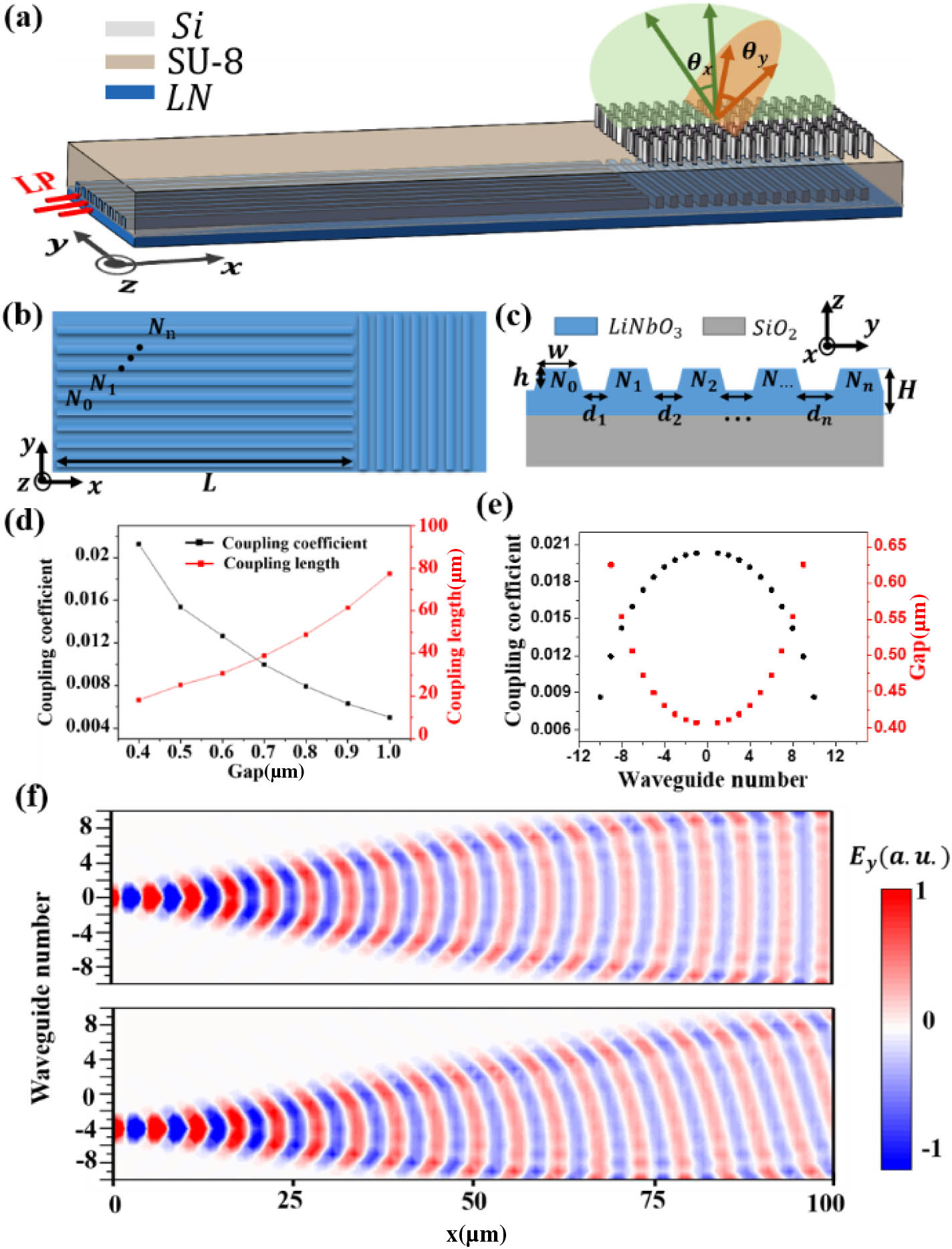
The device is schematically shown in Fig. 1(a), and includes mainly three parts: waveguide arrays, grating radiation antenna, and metasurface. The proposed metasurface-based POPA design for beam steering in two dimensions is shown in Fig. 1(a), and steering the beam in the dimension and dimension can be achieved by switching input waveguides and tuning the wavelength. The metasurface is integrated on top of POPA to enlarge the FOV. Here, the LNOI platform is employed, which contains a 600 nm thick layer of LN film, and a buried layer of with thickness of 2 μm on the Si substrate. Ridge waveguides are designed 600 nm wide, with a 300 nm slab thickness and 300 nm ridge height, and the non-uniform space range of the waveguide array is from 0.4 μm to 0.8 μm. Figures 1(b) and 1(c) show the top and cross-sectional views of the non-uniform waveguide array we designed. The wavefront interferes in the LN slab and emits into space through the grating, so the cross talk between the antennas is negligible, and those features lead to simple manufacturing and small fabrication-induced phase errors.
Figure 1.Design of the metasurface-based POPA on LNOI platform. (a) Scheme of the metasurface-based POPA device for 2D optical beam steering. The output beam can be steered in two dimensions (represented in orange and green). (b) Top and (c) cross-sectional views of the non-uniformly arranged waveguide array without metasurface. (d) Coupling coefficient and coupling length as a function of the gap of waveguides. (e) Simulated coupling coefficient designed and gap distributions for different waveguides. (f) profile input into and waveguides by coupled-mode theory (CMT) calculated in 1D lithium niobate waveguide arrays.
We adopt an aperiodic waveguide array with non-uniform distribution of coupling coefficients [see Fig. 1(e)], i.e., , where is the total waveguide number, indices range from to , and is a scaling factor introduced for experimental reasons. This engineered waveguide array is designed analogous to the matrix elements of the angular momentum -operator, which turns out to be an elaborated definition of the discrete fractional Fourier transform. Consequently, the designed waveguide arrays should be able to transform a point source into a plane wave, i.e., the in-plane Fourier transform [44,45]. The coupling coefficient between two LN waveguides with respect to the waveguide gap can be simulated by using 3D FDTD Solution, as shown in Fig. 1(d). As such, we are able to obtain the waveguide gap distributions in the aperiodic waveguide array [see Fig. 1(e)]. The optical field evolution in this waveguide structure is described by the coupled-mode theory (CMT) where and denote the optical field and propagation constant of the th waveguide, respectively, and is the coupling coefficient between waveguides and . Figure 1(f) shows the CMT calculated light propagation patterns. The input optical field has the form (0.47, 1, 0.47), and it is shown that the field propagates to a uniform intensity distribution around the center waveguides. The input pattern (0.47, 1, 0.47) will give rise to a flatter intensity distribution and phase front at the output by inverse design. Importantly, the wavefront exhibits flat features, and the phase-tilt increases as the input port gradually moves away from the central waveguide [see Fig. 1(e), bottom]. It is evident that our designed aperiodic waveguide array can transform a single waveguide input into a nearly uniform intensity distribution with a flat wavefront, which gives rise to the point-selected phase difference.
In simulations, a 21-waveguide array is chosen in modeling through a 3D FDTD Solution. The input is a TE mode defined by placing the sources at the fifth, sixth, and seventh waveguides with an amplitude ratio of 0.47:1:0.47 to satisfy required input amplitudes. As shown in Fig. 2(a), the simulated electrical field distribution for light propagation in the waveguide array and emitting antenna region validates that the radiated waves have a uniform amplitude distribution in the emitting antenna region. To confirm the phase distribution, we simulated the profile of the emitting antenna region at μ, and it is clear that the tilted phase is consistent with the phase we designed [Fig. 2(b)]. In addition, Fig. 2(c) shows the profile of the plane at μ, which indicates the tilted phase from waveguide emission to space.
Figure 2.(a) Simulated electrical field distribution for light propagation in waveguide array and emitting antenna region. (b) profile of the μμ emitting antenna region at μ. (c) profile of plane at μ for light emitting from grating incidence to space.
In experiments, to further improve the resolution of beam steering, we implemented an OPA device employing 41 waveguides, and the propagation length from the input to the radiating antenna was μ. The SEM images of the coupling grating, waveguide array structure, and emitter antenna are shown in Fig. 3(a). The performance of the OPA was measured using a Fourier-space imaging system with an objective lens of and an infrared sensor camera (XenicsXeva-1.7-320) (see Appendix A for details). From Fig. 3(b), the far-field spot size of port -2 is without sidelobes at the wavelength of 1550 nm measured by a Fourier-space imaging system. The POPA far field and line profile by switching from port -6 to port 6 are shown in Fig. 3(c). The optical intensity is concentrated mainly in the main lobe without any sidelobes in the range of , which indicates that the power is concentrated on the main lobe and the POPA, which gives rise to aliasing-free beam steering. In fact, we fabricated another sample with 21 waveguides the same as the theoretical simulation (not shown here). It is found that the FWHM of this 41-waveguide OPA decreases from 5.07° to 2.74° in the dimension as compared with the 21-waveguide one, revealing the improved resolution. In addition, when we sweep the wavelength from 1470 nm to 1565 nm, we achieve a 7.06° scanning range (see details in Appendix B).
Figure 3.Experiments of POPA on LNOI and beam steering results. (a) Scanning electron microscopy (SEM) image and zoom-in regions of the POPA sample. The sample consists of an array of 41 waveguides, 12 grating couplers connected to the array, and the radiating grating. Top right inset shows the splitter. Bottom right inset shows the distribution of waveguides in the array. (b) Measured far-field intensity pattern of the POPA with an FWHM beam size of and corresponding far-field image captured by the near-infrared camera at port -2. Right inset shows the full 2D far-field image of the beam spot. (c) Measured optical power versus angle at different angles in direction, showing a viewing angle (marked with different colors); right inset shows composition of far-field patterns from 12-port switching.
To expand the scanning angle, a metasurface-based POPA was subsequently implemented on the LNOI platform, as schematically shown in Fig. 4(a), where a well-designed metasurface is integrated on top of the OPA grating with a buffer layer. The metasurface is an array of subwavelength antennas with spatially varying geometric parameters to locally modulate the optical response, so as to flexibly manipulate the phase, polarization, and propagation of light. Here, a polymer (SU-8) layer was spin-coated to fill the waveguide gaps and cover the grating, and to act as a buffer layer to protect the structure of POPA. Then, amorphous Si nanopillars as metasurface components are distributed on the SU-8, where the unit cell is schematically shown in Fig. 4(b). The rectangular nanopillar units are designed with sizes of at a height of 1 μm and arranged in a square lattice with a period of 800 nm. Light travels in the waveguide with TE mode corresponding to linear polarization (LP), which can decompose into left-circular polarization (LCP) and right-circular polarization (RCP). In the experiment, we design the metasurface to deflect the LP light into RCP and LCP with two different output directions. The deflection is obtained by using a geometric phase that results from the polarization conversion of radiation light [32,33]. The metasurfaces will not only convert the LP into LCP and RCP, but also add a spatial phase term based on their orientation angles. The simulated polarization conversion rate (PCR) is as high as for the unit structure to guarantee high efficiency at the incident angle of 0° [see Fig. 4(c) and Appendix C]. We chose a horizontal phase gradient to deflect the radiation light from POPA into the desired angle. According to the generalized Snell law of refraction [32], where is the radiation angle of POPA; is the angle of refraction; is the refractive index of SU-8; is the refractive index of air; ; introduces a phase gradient to increase the angles of refraction for RCP and LCP, respectively. So, the radiation angle writes as
Figure 4.(a) Illustration of the Si metasurface integrated on the region of LNOI grating with geometric phase. (b) Schematic of the integrated metasurfaces’ optical antenna for POPA. (c) Numerically simulated phase shifts (RCP and LCP) and polarization conversion rate (PCR) as a function of rotation angle of a meta-atom, driven by a guide wave with LP. (d) Deflection beam angle versus the incident angle without or with metasurfaces.
Because of the change of the ambient medium of POPA (from air to SU-8), the angle of radiation into air decreases from 21.27° to 19.13°. As the meta-induced deflection angle introduced by metasurfaces is a constant within of the incident angle, the linear phase gradient we designed introduces deflection of about 20° to meet the angle expansion and the steering of the whole FOV [Fig. 4(d)]. According to theoretical calculation, if the in-plane incident angle range can meet , the FOV of a metasurface empowered OPA would possibly reach 180°, which is an extremely high value in OPA scanning range. We also theoretically calculated the diffraction efficiency of the metasurface by 3D FDTD Solution (), and the working efficiency of the final device in the experiment was about 1.7%.
In experiments, we fabricated the metasurface by using electron-beam lithography (EBL, Elionix ELS-F125) and dry etching, as the SEM images of samples show in Figs. 5(a) and 5(b) (see Appendix D for the detailed fabrication process). According to the above calculation, the scanning angle range is beyond , which is out of the of the objective lens; we then slightly shifted the objective lens downside to observe the complete steering angle in a negative axis. Figure 5 illustrates the images from the near-infrared camera together with the measured data. One may notice that the far field is dual-beam intensity distribution on the lateral axis coupled into the 14 input ports. The maximum angle beam of was measured in the negative axis, while that in the positive axis is only 34.2° due to the limitation of NA [see Fig. 5(d)]. By rotating the polarizer and quarter-wave plate, the RCP and LCP beams will be separately observed, as shown in the Figs. 5(e) and 5(f), respectively. Here, we chose the output data from port -6 to analyze the performance of metasurface-based POPA; the peak-to-sidelobe ratios of RCP and LCP are and , respectively. In fact, the only sidelobe is composed of transmitted light not modulated by metasurfaces, so its vertical coordinate is always in the center of RCP and LCP, and the modulation efficiency will also be affected by the phase gradient. Note that there is some background noise in the far field and line profile, i.e., noise between and in Figs. 5(e) and 5(f). It is due to the noise from the grating couplers captured by the objective lens in experiments, since the distance between the input grating coupler and the radiating antenna is less than 0.5 mm in our device. Undoubtedly, the whole performance can be improved by further optimization.
Figure 5.(a), (b) SEM images of the fabricated metasurface structure in the experiment. (c) Steered beams quantized by the normalized intensity distribution from the different incident ports with different colors. (d) Fourteen slices of beam profiles of the far-field image with different input ports stitched together to show beam steering, in which the boxed port -6 case is highlighted for detailed analyses. (e), (f) Measured far-field emission pattern of port -6_RCP and port 6_LCP, demonstrating and peak-to-sidelobe ratio for the beam pointing toward ().
We have proposed a metasurface-based OPA on the LNOI platform with independent port-selection, which definitely shows the capability of free-space beam steering across FOV, aliasing-free. In our approach, a non-periodic -waveguide array is employed to achieve a flat phasefront sweeping in an aliasing-free manner. By imparting a metasurface design, the lateral scanning range of the aliasing-free POPA beam is doubled (up to ) with background suppression of . The dual-beam scanning will not only ensure a wide FOV, but also improve the frame rate. In addition, we could employ a tunable liquid crystal polarizer to filter out one branch to return to single beam scanning to avoid the problem of cross talk without a decrease in the sweeping angle range. Note that though the current device works in a static scheme, it is possible to realize a dynamic scanning of POPA by using Mach–Zehnder interferometer (MZI) switches. In this regard, the excellent EO modulation and low-loss property of the LN waveguide promise high potential advantage for high-speed OPA technology. This work provides a successful demonstration by incorporating the metasurface design into OPA, which can open a new degree of freedom to achieve aliasing-free beam steering and FOV enlargement.
Acknowledgment
Acknowledgment. T. Li is grateful for the support from the Dengfeng Project B of Nanjing University.
APPENDIX A: EXPERIMENT SETUP
A schematic of the experimental setup for near-field and far-field imaging measurements is shown in Fig. 6. A free-space laser beam modulated by a linear polarizer was focused by objective 1 () and then coupled into the sample. The light emitted from the radiation grating is collected by a high objective and imaged in an intermediate imaging plane prior to detection with a near-infrared camera in either the near field or far field (green and red paths in Fig. 6, respectively). For convenience, we will use the terms near-field imaging and far-field imaging to refer to imaging in real space and in Fourier space, respectively. Objective 2 performs the Fourier transform of the object plane into the Fourier plane, and lens L1 performs another Fourier transform and creates an image in the intermediate image plane, allowing spatial filtering. Switching between the near-field and far-field images is accomplished by removing only the optical lens L3: either the intermediate image plane or the Fourier plane is imaged on the CCD array with and without lens L3, respectively. In a metasurface-based POPA device, the RCP and LCP beams will be separately observed by adding a quarter-wave plate and polarizer.
Figure 6.Schematic of the experimental setup for near-field and far-field imaging measurements. The extracted light in free space was collected by objective 2 () and then transmitted through tube lens 1, lens 2, and lens 3. The red path corresponds to near-field imaging, and green corresponds to far-field imaging with L3 removed. A plate and a linear polarizer are used to observe RCP and LCP beams in the metasurface-based POPA, separately.
Longitudinal sweeping characteristics: in the longitudinal direction, different emissions are achieved by adjusting the wavelength. The longitudinal emission angle is given by where is the effective index of the waveguide within the grating for , is the grating pitch, and is the free-space wavelength. As shown in Fig. 7, the wavelength changes from 1470 nm to 1565 nm, and the emssion angle in direction is deflected from to 0.96° achieving a 7.06° scan range. During the entire wavelength adjustment process, the background noise increases due to the best coupling angle of the grating being changed.
Figure 7.Normalized far-field pattern along the axis for wavelengths from 1470 nm to 1565 nm.
Here, we choose rectangular α-Si nanopillars with height 1 μm and widths and as the nanostructure. The simulations were performed with the three-dimensional (3D) FDTD Solution method by using commercial FDTD software (Lumerical). The - and -polarization plane waves were illuminated from SU-8 to the nanopillar arranged in a square lattice. A library that determines the relation between the phase shifts and the dimensions of the nanostructures is established by a parameter sweep at the designed wavelength. The widths and ranged from 200 nm to 400 nm with a lattice constant of 800 nm. Figures 8(a) and 8(b) show the simulated phase shifts and intensities of the transmission coefficients, respectively. The average PCR is about 99.9% for LCP to RCP as the incident angle increases from 0° to 25° with and [Fig. 8(d)]. The PCR is defined as , where and represent the complex transmission coefficients of cross-polarized and co-polarized light, respectively. We also simulated that the transmission decreased to 81.5% when the incident angle was increased to 25°.
Figure 8.Simulation data for 2D parameter sweeps of α-Si nanopillars with height of 1 μm. (a), (b) Simulated phase shifts and intensity of transmission coefficients of nanostructures for - and -polarization beams with various and . These four graphs constitute the library for the parameters of our metasurface layers. (c) Simulated polarization conversion rate (PCR) of each nanostructure for LCP to RCP. (d) Transmission and PCR versus incident angle.
A commercially available LNOI wafer (available from NANOLN Company) with a 600 nm thick LN device layer and 2.0 μm buried silicon dioxide is first cleaned by sonication in acetone and dried with a stream. A 436 nm thick ma-N2405 is spin coated on LN thin film as a mask, and waveguide patterns are defined by an E-beam lithography (EBL) system subsequently. The patterns are transferred 300 nm deep into LN with an optimized argon plasma in an inductively coupled plasma (ICP) etching system (Oxford Plasma Pro 100 Cobra 300). After LN sidewall cleaning and mask removal, a 1.0 μm thick α-Si film is then deposited on the top surface of the SU-8 by plasma-enhanced chemical vapor deposition (PECVD). Subsequently, a positive electron beam resist (PMMA) is spin-coated and followed by the EBL process to define the metasurface and coupler patterns. After development, a 30 nm thick chromium (Cr) film is deposited onto the wafer using electron-beam evaporation, followed by overnight lift-off to transfer the patterns. Then the patterned chromium layer serves as a hard mask for dry etching the Si film in a mixture of and plasma (HSE200S, Naura). Finally, the remaining chromium mask is removed by ammonium cerium nitrate (Fig. 9).
Figure 9.Procedure for fabricating the proposed metasurface-based POPA device.
Zhizhang Wang, Wange Song, Yuxin Chen, Bin Fang, Jitao Ji, Haoran Xin, Shining Zhu, Tao Li, "Metasurface empowered lithium niobate optical phased array with an enlarged field of view," Photonics Res. 10, B23 (2022)