
Jing Long, Binzhang Jiao, Xuhao Fan, Yuncheng Liu, Leimin Deng, Liangti Qu, Wei Xiong. Femtosecond Laser Assembly of One-Dimensional Nanomaterials and Their Application[J]. Chinese Journal of Lasers, 2021, 48(2): 0202017
- Chinese Journal of Lasers
- Vol. 48, Issue 2, 0202017 (2021)
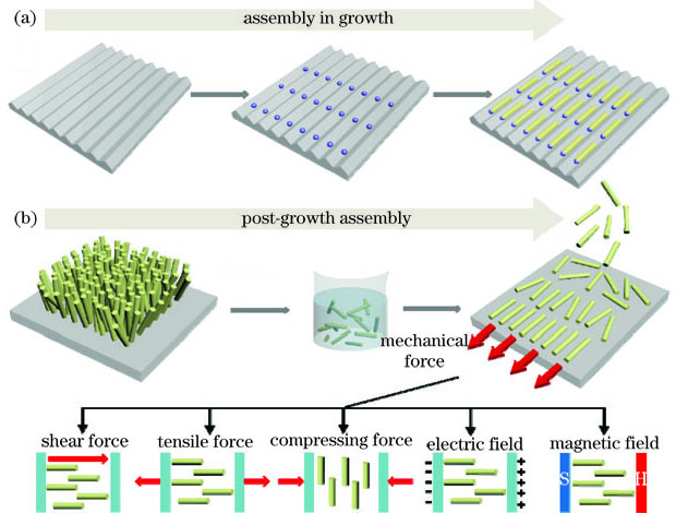
Fig. 1. Traditional assembly methods of 1D nanomaterials. (a) In-situ assembly method; (b) post-growth assembly method
![Assembly technology of 1D nanomaterials based on non-laser direct writing. (a) Template assisted method[28]; (b) fluid-flow method[7]; (c) contact printing method[8]; (d) stretching technique[23]; (e) LB technique[9,29]<](/richHtml/zgjg/2021/48/2/0202017/img_2.jpg)
Fig. 2. Assembly technology of 1D nanomaterials based on non-laser direct writing. (a) Template assisted method[28]; (b) fluid-flow method[7]; (c) contact printing method[8]; (d) stretching technique[23]; (e) LB technique[9,29]<
Fig. 3. Femtosecond laser fabricated Au nanowire aggregate microstructures[44]. (a) Schematic of formation of Au nanowire aggregation and its mechanism; (b) morphologies of laser fabricated aggregates of Au nanowires doped photoresist under different laser power densities
Fig. 4. Femtosecond laser assembled Au nanorods[45]. (a) Schematic of laser assembly of Au nanorods; SEM images of (b) Transformers car logo and (c) spiral ring; microstructural morphologies of Au nanorods fabricated under laser powers of (d)10mW, (e) 25mW, and (f) 40mW
Fig. 5. Two-color laser printing of individual Au nanowire[46]. (a) Schematic of two-color laser printing setup; (b) schematic of laser trapping and aligning of Au nanowires; (c) normalized extinction spectrum of PEG decorated Au nanowires; SEM images of (d) “O” and (e) “X” patterns of printed Au nanowires; dark-field white light Rayleigh scattering images of “OX” patterns excited by (f) non-polarized laser, (g) vertically polarized laser, and (h) horizo
Fig. 6. Ag NWs thiol functionalization and ATA composite micro/nanostructures[47]. (a) Schematic of Ag NWs thiol functionalization; (b) TEM image of thiol-capped Ag NWs; (c) mass spectra of structures fabricated using pure acrylate and ATA composite; SEM images of (d) spiral-like photonic crystal, (e) micro-coil, and (f) micro-capacitor
Fig. 7. Laser nano-joining of Ag NWs within ATA composites[47]. (a) Schematic of laser nano-joining of Ag NWs junctions including three processes of initiation, activation, and diffusion; TEM images and crystal lattice diffraction images of Ag NW junctions (b) before and (c) after laser irradiation fusion; (d) magnified TEM image of fused Ag NW junctions; (e) scheme of welding two Ag NWs over (111) growing plane
Fig. 8. Femtosecond laser direct writing of SWNTs/polymer composites[13]. (a) Schematic of femtosecond laser direct writing of 3D SWNTs/polymer composites; (b) SEM images and schematic of stereo structures made of nanowire arrays; (c) polar-diagram of G-band relative intensity versus angle between laser polarization direction and scanning direction; (d) schematic and (e) SEM image of alignment of suspended cantilever structure; (f) polar-diagram of G-ban
Fig. 9. Femtosecond laser direct writing and assembly of MWTNs[50]. (a) Experimental setup of TPP fabrication; (b) comparison of polymerized MA photoresist (down) and MTA photoresist (up); (c) comparison of newly fabricated MTA photoresist and that after one week; (d) TPP fabricated Au electrode pattern on flexible PET substrate; SEM images of (e) micro-coil inductor, (f) micro-pyramid, (g) spiral photonic crystal, (h) micro-capacitor array, and (i) micr
Fig. 10. Electrical and mechanical performance characterization of femtosecond laser assembled MWNTs[51]. (a) SEM micrograph of MWNTs micro-line structure after annealing; (b) polar-diagram of G-band relative intensity versus angle between laser polarization direction and micro-wire axial direction; (c) SEM micrographs of long rectangle bars fabricated under different laser scanning directions; (d) current-voltage characteristic curves of long rectangle b
Fig. 11. Femtosecond laser direct writing and fabrication of ZnO NWs/polymer composite micro/nanostructures [61]. (a) ZnO NWs/polymer stereo microstructures with different doping concentrations; (b) photoelectron spectra of ZnO NWs/polymer composite micro/nanostructures; (c) Raman spectra of ZnO NWs powder (i), pure resin polymer micro/nanostructures (ii) , and ZnO NWs/polymer composite micro/nanostructures (iii); (d) fluorescence spectra of ZnO NW powder
Fig. 12. Femtosecond laser direct writing and assembly of ZnO NWs [62]. (a) Comparison of pure acrylate resin and ZNA composite resin; (b) water contact angle diagrams of ZnO NWs before and after silane modification; (c) SHG spectra of pure acrylate resin and ZNA composite resin; (d)(e) schematic diagrams of femtosecond laser assembly of ZnO NWs; (f) SEM images of ZNA composite micro/nanostructures, including spiral photonic crystal and visual-ring
Fig. 13. Alignment characterization of ZnO NWs in ZNA composite micro/nanostructures[62]. (a) Optical micrograph of ZNA flower pattern; (b) P-SHG polar-diagram and (c)(d) mapping images of ZNA flower pattern; (e) SEM images of ZNA (e) grid and (f) woodpile structures after high temperature thermal treatment and upper right corner is SEM image before annealing of woodpile structure
Fig. 14. Femtosecond laser assembly of Au nanorods used for SERS detection [45]. (a) Schematic of SERS detection of microfluidic chip based on Au nanorod micro/nanostructure; (b) Raman spectrum of R6G probe molecules
Fig. 15. Temperature-dependent electrical conductivity characterization of ATA composite micro/nanostructures [47]. (a)Schematic and (b) setup for electrical conductivity test; (b) current-voltage curves of ATA composite structure and pure pure acrylate resin under laser welding and 523 K; (d) temperature-dependent electrical conductivity of ATA composite micro/nanostructure
Fig. 16. TPP-based femtosecond laser direct writing and fabrication of MWNTs-based functional devices [50]. (a) SEM image of MWNTs composite polymer array after vacuum thermal annealing and magnified SEM image of assembled MWNT bundle shown in inset; (b) current-voltage curves of MWNTs composite polymer line array before and after thermal annealing; (c) optical micrograph of capacitor array between two Au electrodes and SEM image of single capacitor shown
Fig. 17. ZnO NWs-based polarized UV photodetectors fabricated by TPP-based femtosecond laser direct writing [62]. (a) Schematic; (b)optical micrograph; (c) time-resolved response of device; (d) photocurrents of device under different UV polarization angles
Fig. 18. Alignment intensity characterization of SWNTs in SWNTs/polymer composite microstructures[13]. (a) SEM images of suspended nanowires with different wire widths; (b) nematic order parameter versus wire width; (c) SEM images of micro-cubes fabricated along mutually perpendicular laser scanning direction, in which left cube is made of NWs arranged along x-axis and right cube is made of NWs arranged along y-axis; (d) structural diagram o
Fig. 19. Schematic of femtosecond laser assembly of ZnO NWs [62]. (a) Schematic of assembly mechanism; (b) square structures fabricated under different laser scanning routes and polarization directions and their polarized SHG mapping images

Set citation alerts for the article
Please enter your email address
© Copyright 2018-2021 | Chinese Laser Press. All Rights Reserved 沪ICP备15018463号-20