
Jinhua Zhao, Xueshuai Jiao, Yingying Ren, Jinjun Gu, Sumei Wang, Mingyang Bu, Lei Wang, "Lithium niobate planar and ridge waveguides fabricated by 3 MeV oxygen ion implantation and precise diamond dicing," Chin. Opt. Lett. 19, 060009 (2021)
- Chinese Optics Letters
- Vol. 19, Issue 6, 060009 (2021)
Abstract
1. Introduction
Lithium niobate (
Since ion implantation has become an effective and relatively mature waveguide manufacturing tool in the past decades[
Sign up for Chinese Optics Letters TOC. Get the latest issue of Chinese Optics Letters delivered right to you!Sign up now
The optical waveguide has become the basic component for electro-optic devices in PICs. In particular, two-dimensional (2D) waveguides[
2. Experiment and Details
The LN crystals used in this work are
2.1. Planar waveguide formation and optimization
To obtain a low loss planar waveguide, O ions at the energy of 3.0 MeV with a fluence of
2.2. Precise dicing and ridge waveguide formation
The precise dicing technique is used to carve grooves in LN planar waveguides. This process is completed in Shanghai (Disc DAD323). The important criteria for obtaining an eligible ridge are smooth side walls and little chipping on both the surface and end face. Ridge waveguides with smooth walls and acceptable edges are fabricated by adjusting the dicing conditions. The optimum dicing condition used in this work is that the thickness and diameter of the diamond blade are 23 µm and 56 mm, respectively, the rotation speed is 40,000 r/min, and the moving speed is 0.5 mm/s. The blade is translated along the entire length of the wafer, which is convinced that the precise dicing is an effective and useful tool to fabricate centimeter-long ridge waveguides. The near-field intensity profile and propagation loss of ridge waveguides are measured by the end-face coupling method.
3. Results and Discussion
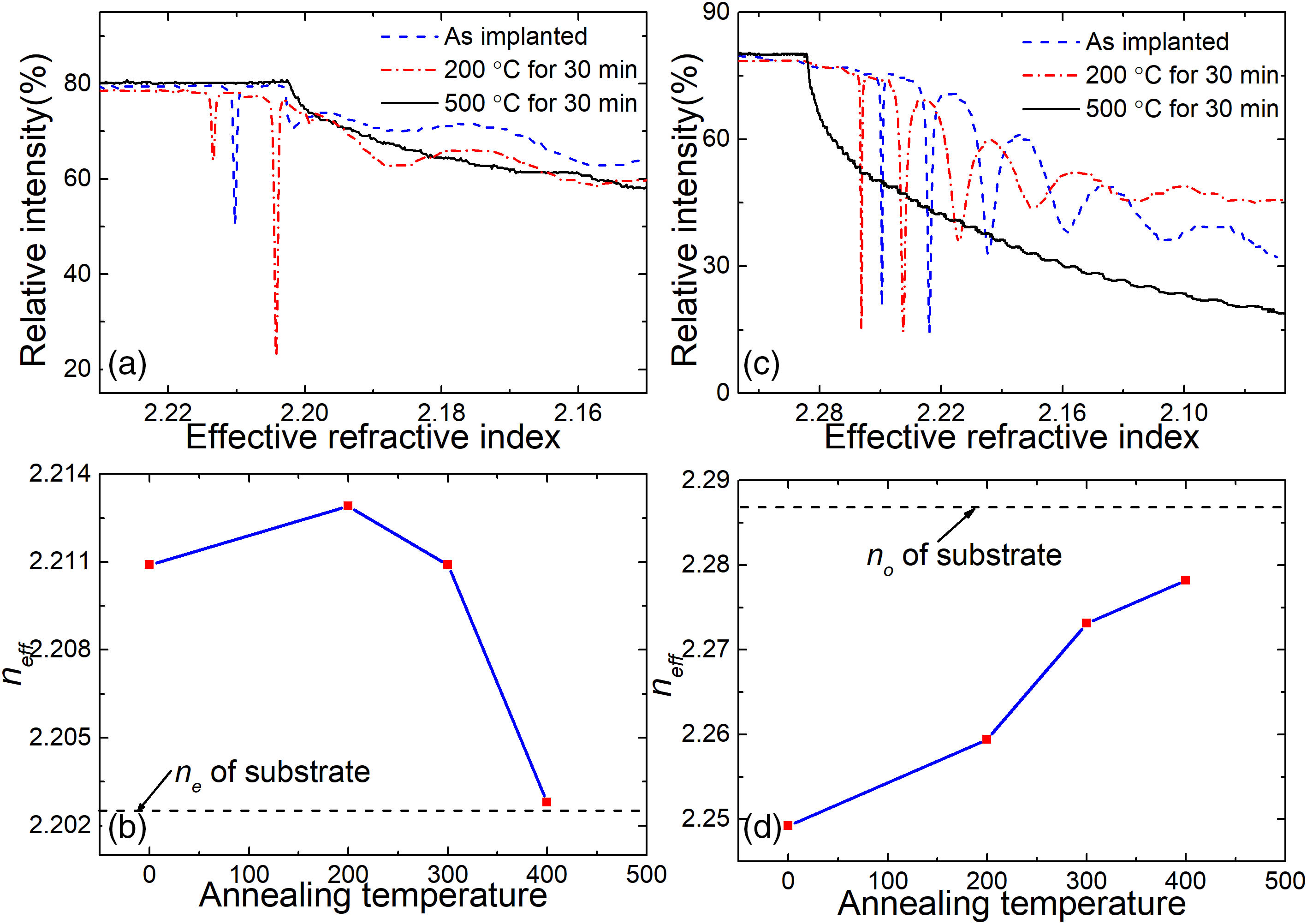
The values of the substrate refractive index (
![]()
Figure 1.Measured relative intensity of reflected light from the prism versus the effective refractive index at a wavelength of 633 nm before and after annealing for O implanted planar waveguides: (a) TM polarized light and (c) TE polarized light. Effective refractive indices of the (b) TM0 mode and (d) TE0 mode varying with different annealing temperatures for the same time of 30 min.
The stopping and range of ions in matter (SRIM) 2013[
![]()
Figure 2.Dpa profile of the 3 MeV O ions with the fluence of 1.5 × 10¹⁵ ions/cm2 implanted into LiNbO3 crystal.
![]()
Figure 3.Reconstructed RIP of the LiNbO3 planar waveguide at a wavelength of 633 nm after A1 annealing treatment: (a) TE; (b) TM.
The end-face coupling method is utilized to investigate the guiding properties and propagation loss of waveguides at a wavelength of 633 nm. The experimental results indicate that the waveguide could not carry the TE mode, which is due to the weak limit of light for the optical barrier. In addition, the O implanted waveguide could carry the TM mode; however, the loss of the
![]()
Figure 4.Near-field intensity profiles of the LiNbO3 planar waveguide at a wavelength of 633 nm after A2 annealing treatment: (a) measured by the end-face coupling method; (b) calculated by the beam propagation method.
Based on the above analysis, the planar waveguide at the
| Waveguide | Loss (dB/cm) |
|---|---|
| WG15 | 4.5 |
| WG25 | 2.4 |
| WG35 | 1.5 |
| WG50 | 1.0 |
Table 1. Propagation Losses of the Ridge Waveguides WG15–WG50 at a Wavelength of 633 nm for TM Polarization
![]()
Figure 5.Optical microscope images of ridge waveguide cross section: (a) WG15; (b) WG25; (c) WG35; (d) WG50.
![]()
Figure 6.Near-field intensity profiles of the LiNbO3 ridge waveguide with a width of 15 µm at the wavelength of 633 nm: (a) measured by the end-face coupling method; (b) calculated by the beam propagation method.
In the following part, we will focus on the relationship between propagation loss of the waveguide and RIP for medium-mass ion implantation at the energy of MeV. According to the related research in the previous work, we know that the waveguide formation is attributed to the enhanced-index well and optical barrier. In LN crystal, the enhanced-index well is formed by an appropriate reduction of spontaneous polarization, and this reduction will raise the extraordinary refractive index and decrease the ordinary refractive index. This can explain the variation of the surface refractive index (
4. Conclusions
In conclusion, with the ion implantation and precise dicing of LN crystals, we have achieved planar and ridge waveguides with acceptable propagation loss. The mode profiles and propagation loss of planar and ridge waveguides have been investigated in detail. The optimum annealing treatment was obtained in this work under our implanted condition. The relationship between the propagation loss of the waveguide and RIP for medium-mass ion implantation at the energy of MeV is clarified. The propagation loss of WG15 is 4.5 dB/cm, and, with the increase of the waveguide width, propagation losses decreased to 2.4 dB/cm, 1.5 dB/cm, and 1.0 dB/cm, respectively. The reason for this may be that chipping the side walls is a critical factor for large propagation loss of the ridge waveguide, especially when the width of the ridge is equal to or less than 15 µm. Our work will provide reference data for the application of LN crystals in integrated photonic devices.
References
[1] M. Digonnet, M. Fejer, R. Byer. Characterization of proton-exchanged waveguides in MgO:LiNbO3. Opt. Lett., 10, 235(1985).
[2] P. J. Chandler, L. Zhang, J. M. Cabrera, P. D. Townsend. “Missing modes” in ion-implanted LiNbO3 waveguides. Appl. Phys. Lett., 54, 1287(1989).
[3] G. Poberaj, H. Hu, W. Sohler, P. Günter. Lithium niobate on insulator (LNOI) for micro-photonic devices. Laser Photon. Rev., 6, 488(2012).
[4] C. Pang, R. Li, Z. Q. Li, N. N. Dong, J. Wang, F. Ren, F. Chen. Multi-gigahertz laser generation based on monolithic ridge waveguide and embedded copper nanoparticles. Chin. Opt. Lett., 19, 021301(2021).
[5] P. D. Townsend, P. J. Chandler, L. Zhang. Optical Effects of Ion Implantation(1994).
[6] F. Chen, X.-L. Wang, K.-M. Wang. Development of ion-implanted optical waveguides in optical materials: a review. Opt. Mater., 29, 1523(2007).
[7] H. Hu, F. Lu, F. Chen, B. R. Shi, K. M. Wang, D. Y. Shen. Extraordinary refractive-index increase in lithium niobate caused by low-dose ion implantation. Appl. Opt., 40, 3759(2001).
[8] L. Wang, F. Chen, X. L. Wang, L. L. Wang, K. M. Wang, L. Gao, H. J. Ma, R. Nie. Si2+ ion implanted into stoichiometric lithium niobate crystals: waveguide characterization and lattice disorder analysis. Nucl. Instru. Meth. Phys. Res. B, 251, 104(2006).
[9] G. G. Bentini, M. Bianconi, L. Correra, M. Chiarini, P. Mazzoldi, C. Sada, N. Argiolas, M. Bazzan, R. Guzzi. Damage effects produced in the near-surface region of x-cut LiNbO3 by low dose, high energy implantation of nitrogen, oxygen, and fluorine ions. J. Appl. Phys., 96, 242(2004).
[10] Y. Tan, F. Chen, D. Kip. Photorefractive properties of optical waveguides in Fe:LiNbO3 crystals produced by O3+ ion implantation. Appl. Phys. B, 94, 467(2009).
[11] J. Zhang, Y. Zhang, J. Xu, S. B. Lin, C. X. Liu. Planar and ridge waveguides formed by proton implantation and femtosecond laser ablation in fused silica. Vacuum, 172, 109093(2020).
[12] H. Hu, R. Richen, W. Sohler. Low-loss ridge waveguides on lithium niobate fabricated by local diffusion doping with titanium. Appl. Phys. B, 98, 677(2010).
[13] J. H. Zhao, X. H. Liu, Q. Huang, P. Liu, X. L. Wang. Lithium niobate ridge waveguides fabricated by ion implantation followed by ion beam etching. J. Lightwave Technol., 28, 1913(2010).
[14] G. Ulliac, B. Guichardaz, J. Y. Rauch, S. Queste, S. Benchabane. Ultra-smooth LiNbO3 micro and nano structures for photonic applications. Microelectron. Eng., 88, 2417(2011).
[15] S. Siew, E. Cheung, H. Liang, A. Bettiol, N. Toyoda, B. Alshehri, E. Dogheche, A. Danner. Ultra-low loss ridge waveguides on lithium niobate via argon ion milling and gas clustered ion beam smoothening. Opt. Express, 26, 4421(2018).
[16] M. Qu, Y. Shen, L. Wu, X. Fu, X. Cheng, Y. Wang. Homogenous and ultra-shallow lithium niobate etching by focused ion beam. Precision Eng., 62, 10(2020).
[17] Y. Cheng, J. Lv, S. Akhmadaliev, S. Zhou, Y. Kong, F. Chen. Mid-infrared ridge waveguide in MgO:LiNbO3 crystal produced by combination of swift O5+ ion irradiation and precise diamond blade dicing. Opt. Mater., 48, 209(2015).
[18] A. Caspar, M. Roussey, M. Häyrinen, J. Laukkanen, A. Pérignon, F. Behague, V. Calero, G. Ulliac, M. Bernal, M. Kuittinen, N. Courjal. High-aspect-ratio LiNbO3 ridge waveguide with vertical buffer layer and enhanced electro-optical efficiency. J. Lightwave Technol., 36, 2702(2018).
[19] A. Gerthoffer, C. Guyot, W. Qiu, A. Ndao, M. Bernal, N. Courjal. Strong reduction of propagation losses in LiNbO3 ridge waveguides. Opt. Mater., 38, 37(2014).
[20] D. Brüske, S. Suntsov, C. Rüter, D. Kip. Efficient Nd:Ti:LiNbO3 ridge waveguide lasers emitting around 1085 nm. Opt. Express, 27, 8884(2019).
[21] L. Wang, C. Haunhorst, M. Volk, F. Chen, D. Kip. Quasi-phase-matched frequency conversion in ridge waveguides fabricated by ion implantation and diamond dicing of MgO:LiNbO3 crystals. Opt. Express, 23, 30188(2015).
[22] Y. F. Niu, L. Yang, D. J. Guo, Y. Chen, X. Y. Li, G. Zhao, X. P. Hu. Efficient 671 nm red light generation in annealed proton-exchanged periodically poled LiNbO3 waveguides. Chin. Opt. Lett., 18, 111902(2020).
[24] P. J. Chandler, F. L. Lama. A new approach to the determination of planar waveguide profiles by means of a non-stationary mode index calculation. Opt. Acta, 33, 127(1986).
[25] R. Ramponi, R. Osellame, M. Marangoni. Two straightforward methods for the measurement of optical losses in planar waveguides. Rev. Sci. Instrum., 73, 1117(2002).
[26] L. Wang, F. Chen, X. L. Wang, K. M. Wang, Y. Jiao, L. L. Wang, X. S. Li, Q. M. Lu, H. J. Ma, R. Nie. Low-loss planar and stripe waveguides in Nd3+-doped silicate glass produced by oxygen-ion implantation. J. Appl. Phys., 101, 053112(2007).
[28] J. H. Zhao, Q. Huang, P. Liu, X. L. Wang, H. J. Ma, R. Nie. Annealing behavior of LiNbO3 planar waveguides formed by oxygen ion implantation. Nucl. Instru. Meth. Phys. Res. B, 272, 116(2012).


Set citation alerts for the article
Please enter your email address

© Copyright 2018-2021 | Chinese Laser Press. All Rights Reserved 沪ICP备15018463号-20