Abstract
We report an 8-channel wavelength-mode optical pulse interleaver on a silicon photonic chip. Wavelength- and mode-division multiplexing techniques are combined to increase the repetition rate of the pulses without adding the complexity of a single dimension. The interleaver uses a cascaded Mach–Zehnder interferometer architecture as a wavelength-division (de)multiplexer, an asymmetric directional coupler as a mode (de)multiplexer, and various lengths of silicon waveguides as delay lines. A pulse sequence with a time interval of 125 ps is implemented with the repetition rate being eight times that of the initial one. The demonstrated wavelength-mode multiplexing approach opens a new route for the generation of high-speed optical pulses.Techniques for generation, control, and processing of optical pulses are becoming increasingly important in many scientific fields, including photonic signal processing[1,2], ultrafast sampling[3], arbitrary waveform generation[4], and frequency metrology[5]. Ultrafast sampling based on high-speed optical pulses is demanded in optical analog-to-digital conversion (OADC) systems, as its jitter is several orders of magnitude lower than that of an electronic analog-to-digital converter[6]. The sampling rate of OADC systems is determined by the optical pulse repetition rate. Pulse sequences can also be used for arbitrary waveform generation (AWG)[4] by an independent manipulation of the amplitude and phase of individual lines. High-repetition-rate AWG can find rich applications in high-speed coherent communications[7], quantum optics[8], and medical imaging and instrumentation systems.
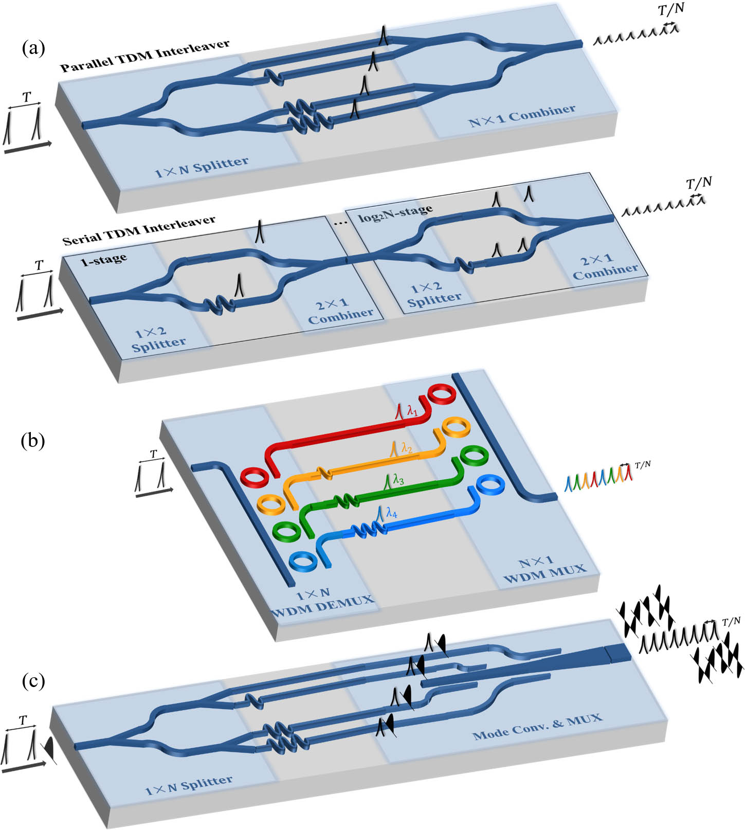
These examples illustrate that there is a high demand for a pulse sequence with a high repetition rate. It is quite challenging to directly generate a high-repetition-rate pulse sequence. Instead, optical multiplexing methods can be used to interleave optical pulses, therefore raising the pulse repetition rate from a low one. Optical time-division multiplexing (TDM) is one of the multiplexing techniques commonly used in optical communications[9–11]. The bit rate of the serialized data stream is the product of the bit rate of a single channel and the number of parallel channels. TDM interleaves the pulses from parallel channels by adjusting their relative time delay using optical delay lines, as shown in Fig. 1(a). In addition to the parallel configuration, the serial TDM structure can also be used to interleave the optical pulses[12]. In each stage, the input pulse is split into two and enters two branches with different lengths. The time-division pulse interleavers can be made of optical fiber components[13] or planar waveguide devices with more compact footprints[14,15]. However, there is a significant intrinsic loss in the time-division interleavers during optical pulse combination, limiting the number of time channels that can be used. Another common approach is to use wavelength-division multiplexing (WDM)[16,17]. The spectrum of the input pulse sequence is divided into several sub-bands by a wavelength demultiplexer. The separate wavelength channels experience deferential delays before they are combined into one by a wavelength multiplexer, as shown in Fig. 1(b). In this way, the pulse repetition rate is increased without suffering pulse combination loss as in time-division interleavers. The increment factor for pulse repetition rate is limited by the number of WDM channels that the input pulse spectrum can accommodate. The pulse repetition rate can be further increased by combining time-division and wavelength-division interleavers[18].

Figure 1.Schematic structures of (a) the TDM interleavers in parallel and serial configurations, (b) the WDM interleaver, and (c) the MDM interleaver.
Mode-division multiplexing (MDM) has been intensively studied in recent years to improve the spectral efficiency and data rate of optical links[19,20]. For example, a monolithically integrated MDM photonic integrated circuit has been demonstrated in which each mode channel can provide a line rate of 100 Gb/s[21]. The waveguide mode is essentially another orthogonal dimension that is independent of time and wavelength dimensions. Therefore, it is natural to think of making use of MDM as a new freedom to increase the pulse repetition rate. Like wavelength-division interleavers, there is also no intrinsic loss in the mode-division interleavers, as shown in Fig. 1(c).
Sign up for Chinese Optics Letters TOC. Get the latest issue of Chinese Optics Letters delivered right to you!Sign up now
In this work, we propose and experimentally implement a wavelength-mode pulse interleaver to generate a high-repetition-rate optical pulse sequence. Four wavelength and two mode channels are used, leading to an 8-fold increased pulse repetition rate. As far as we know, this is the first time that MDM has been used in pulse interleaving. Compared to the single wavelength-division or mode-division interleaver, the combined interleaver relaxes the channel requirement and therefore it is easier to (de)multiplex channels with low cross talk.
Figure 2(a) shows the schematic structure of the wavelength-mode pulse interleaved photonic signal processing system. The wavelength demultiplexer first divides the spectrum of the input pulse into four sections, each section forming a pulse with a different carrier wavelength. The demultiplexed pulses pass through four parallel waveguide delay lines with an incremental delay of . These delayed pulses are combined into a single path at the output using a wavelength multiplexer. Therefore, a pulse sequence with a time interval of is produced. The pulse sequence is then divided into two branches by an optical splitter. The delay difference between the two paths is . It couples to distinct optical modes in a multimode waveguide, forming mode multiplexing. At this stage, a pulse sequence containing 8 pulses with a delay interval is obtained. The repetition rate of the pulse sequence is increased by 8 times compared to the original input pulse. Various functions such as modulation, sampling, and switching can be performed on these high-repetition-rate pulses. The pulse sequence is divided into 8 output channels through mode and wavelength demultiplexing for parallel processing at a lower speed equal to the input pulse. It should be noted that in principle there is no optical loss during wavelength and mode interleaving.
Figure 2.(a) Schematic structure of a wavelength-mode interleaved photonic signal processing system. (b) The structure of the wavelength demultiplexer based on two-stage cascaded Mach–Zehnder interferometers. (c) The structure of the mode converter and multiplexer.
Figure 2(b) shows the structure of the wavelength demultiplexer consisting of three cascaded asymmetric MZIs. The titanium nitride microheater is integrated on the two arms of the MZI for low loss thermal phase tuning. The MZI of the first stage has an arm length difference of and the MZIs of the second stage have a half-length difference of . The length difference is designed to be 46.7 μm, corresponding to a wavelength interval of 3.3 nm between adjacent channels. The wavelength multiplexer is the same as the demultiplexer in structure except for the reverse optical transmission.
Figure 2(c) shows the structure of the mode converter and multiplexer. The modes from two single-mode input waveguides are coupled to the and modes of an adiabatically tapered bus waveguide, respectively. These high-order modes then propagate in the bus waveguide. For the two directional couplers, the widths of the waveguides are carefully designed to ensure that the effective refractive index of the mode of the input waveguide is equal to that of the mode in the bus waveguide.
Figure 3(a) shows a microscope image of the fabricated chip. The minimum line width of our manufacturing process is 0.18 μm. The input, output, and test ports are connected to grating couplers with a pitch of 127 μm for coupling to a fiber array. TiN-based micro-heaters are connected to the electrical pads positioned along the edge of the chip. The chip was fabricated on a silicon-on-insulator wafer with a top silicon layer thickness of 220 nm and a buried oxide layer thickness of 2 μm using a complementary metal-oxide-semiconductor (CMOS) compatible fabrication process. The chip size is . A commercial fiber array was coupled and attached to the chip by using an index-matched UV adhesive. All electrical pads were wire bonded to a printed circuit board so that voltages could be applied to the chip. Figure 3(b) shows the home-packaged chip.
Figure 3.(a) Optical microscope image of the fabricated chip. (b) A photo of the packaged chip with fiber array coupling and electrical wire-bonding to a PCB.
We first measured the transmission spectra of the wavelength demultiplexer, as shown in Fig. 4(a). The channel spacing is 3.3 nm and the channel bandwidth is 2.33 nm. Micro-heaters have been used to tune the phase shifters in the MZIs to adjust the WDM wavelengths. Figure 4(b) shows the transmission spectrum of the wavelength-division interleaver. The center wavelengths of the four channels are , , , and . The insertion losses are 6.38 dB, 7.05 dB, 5.05 dB, and 7.52 dB, respectively. The variation in the insertion loss is mostly caused by the length difference in the waveguide delay lines. The average waveguide propagation loss is approximately 3.3 dB/ns. The propagation loss of waveguide delay lines is always lower than that of other delay line structures, such as photonic crystal waveguides[22] and ring resonators[23]. It is well known that the silicon waveguide loss mainly comes from the waveguide sidewall roughness induced scattering loss. We recently proposed and demonstrated 60 nm thick silicon waveguides that are less sensitive to sidewall roughness. The propagation loss can be reduced by around 5 times compared with the regular 220 nm thick silicon strip waveguides fabricated with the same technique[24,25].
Figure 4.(a) The transmission spectra of the wavelength demultiplexer. (b) The transmission spectrum of the wavelength-division interleaver. (c) (left) The optical pulse waveforms at the end of the wavelength-division interleaver. (right) The delay error of the optical pulses. The red color indicates the measured pulses and the green color indicates the ideal pulses with a time interval of 250 ps.
We next measured the temporal waveforms of the optical pulses to obtain the delay. A wavelength-tunable CW laser was first modulated by an electro-optic modulator driven by an electrical pulse from a pulse pattern generator to produce the optical pulses. The optical pulses were amplified by an erbium-doped fiber amplifier (EDFA) before they entered the wavelength-division interleaver. By tuning the wavelength of the laser light to , , , and , the pulses experience different delays, as shown in Fig. 4(c). It indicates that the pulse at wavelength experiences the minimum delay while the pulse at wavelength has the maximum delay, consistent with the channel loss measurement. The delay errors between the measured pulses and the ideal pulses are 4.15 ps (1.66%), 1.22 ps (0.49%), , and . The root mean squared delay error is 3.19 ps (1.28%). The delay error is generated due to variations in the waveguide dimensions, which is on the same level as the other reports[3]. It can be reduced by using advanced manufacturing tools with a better waveguide patterning accuracy.
After the wavelength-division interleaver, the repetition rate is increased by 4 times. The optical pulses then go through the subsequent two-channel mode-division interleaver. After processing, the pulse sequence is finally demultiplexed into 8 output channels at a lower speed. The mode in the multimode waveguide is converted to the fundamental mode by the mode demultiplexer and the four wavelength channels are then demultiplexed to output ports , , and . Similarly, the mode in the multimode waveguide is converted to the fundamental mode and output from ports , , , and . Figures 5(a) and 5(b) show the measured transmission spectra of the entire wavelength-mode-division interleaver. The interchannel cross talk is approximately at the channel center wavelength. Figure 5(c) shows the optical pulse waveforms at the end of the wavelength-mode-division interleaver with a measured delay interval of around 125 ps. The calculated delay errors of the optical pulses between the measured pulses and the ideal pulses are 7.35 ps (5.88%), 5.62 ps (4.50%), 3.29 ps (2.63%), 0.01 ps (0.01%), 0.58 ps (0.46%), , , and . The corresponding root mean squared timing error is 4.05 ps (3.24%).
Figure 5.(a) The transmission spectra from output ports , , , and through mode transmission in the multimode waveguide. (b) The transmission spectra from output ports , , , and through mode transmission in the multimode waveguide. (c) (left) The optical pulse waveforms at the end of the wavelength-mode-division interleaver. Dotted curves: the optical pulse through the mode; solid curves: the optical pulse through the mode. (right) The delay error of the optical pulses. The red color indicates the measured pulses and the green color indicates the ideal pulses with a time interval of 125 ps.
Table 1 compares our device with various state-of-the-art integrated pulse interleavers. They are based on the TDM multiplexing method[9,12,25,26] or the WDM method[3]. Our wavelength-mode pulse interleaver has no inherent loss and uses MDM as a new degree of freedom to relax the requirement on WDM devices.
| Multiplexing methods | Integration platform | Account of channels | Delay step (ps) | Delay error (%) | Intrinsic loss* (dB) |
|---|
| Parallel-TDM[9] | Silicon | 8 | 25 | – | 9 |
| Serial-TDM[12] | Silica | 24 | 100 | – | 12 |
| Serial-TDM[26] | InP | 22 | 3.1 | – | 6 |
| Serial-TDM[25] | Silicon | 27 | 10 | – | 3 |
| WDM[3] | Silicon | 4 | 253.8 | 0.35 | 0 |
| WDM+MDM | Our work | 8 | 125 | 3.2 | 0 |
Table 1. Performance Comparison of Several Typical Integrated Pulse Interleavers
In conclusion, we have proposed and implemented a pulse interleaver on the silicon photonics platform. The interleaver combines wavelength and mode multiplexing technologies to get an increased pulse repetition rate. A pulse sequence with a time interval of 125 ps is produced with a delay error of 3.2%. These high-repetition-rate pulses can find many applications, such as high-speed optical communication, ultrafast sampling for OADC, and arbitrary waveform generation. Our chip incorporates dozens of electrical and optical components, including MZI switches, asymmetric directional couplers, micro-heaters, grating couplers, etc. They are monolithically integrated in one silicon photonic chip using CMOS-compatible processes. The silicon photonics integration makes it possible to enable potential low-cost and massive production. In addition, MDM is first used for integrated pulse interleavers, providing additional freedom to manipulate optical pulses.
References
[1] S. Kawanishi. IEEE J. Quantum Electron., 34, 2064(1998).
[2] L. Wang, J. Huang, L. Liu, T. Li. Opt. Express, 25, 12161(2017).
[3] H. Gevorgyan, K. Al Qubaisi, M. S. Dahlem, A. Khilo. Opt. Express, 24, 13489(2016).
[4] Z. Jiang, C.-B. Huang, D. E. Leaird, A. M. Weiner. Nat. Photonics, 1, 463(2007).
[5] S. A. Diddams, D. J. Jones, J. Ye, S. T. Cundiff, J. L. Hall, J. K. Ranka, R. S. Windeler, R. Holzwarth, T. Udem, T. W. Hänsch. Phys. Rev. Lett., 84, 5102(2000).
[6] A. J. Benedick, J. G. Fujimoto, F. X. Kärtner. Nat. Photonics, 6, 97(2012).
[7] R. Proietti, C. Qin, B. Guan, N. K. Fontaine, S. Feng, A. Castro, R. P. Scott, S. J. B. Yoo. J. Opt. Commun. Network., 8, A171(2016).
[8] A. S. Kowligy, P. Manurkar, N. V. Corzo, V. G. Velev, M. Silver, R. P. Scott, S. J. B. Yoo, P. Kumar, G. S. Kanter, Y.-P. Huang. Opt. Express, 22, 27942(2014).
[9] A. A. Aboketaf, A. W. Elshaari, S. F. Preble. Opt. Express, 18, 13529(2010).
[10] Z. H. Yu, Q. Zhang, H. Wang, J. J. Zhang, D. R. Selviah. Opt. Commun., 395, 217(2017).
[11] J. Jing, X. Wang, L. Lu, L. Zhou, H. Shu, X. Wang, J. Chen. J. Phys. D, 52, 194001(2019).
[12] M. Y. Sander, S. Frolov, J. Shmulovich, E. P. Ippen, F. X. Kärtner. Opt. Express, 20, 4102(2012).
[13] H.-G. Weber, M. Nakazawa. Ultrahigh-Speed Optical Transmission Technology(2007).
[14] S. Cao, J. Chen, J. N. Damask, C. R. Doerr, L. Guiziou, G. Harvey, Y. Hibino, H. Li, S. Suzuki, K. Y. Wu, P. Xie. J. Lightwave Technol., 22, 281(2004).
[15] L. Zhou, X. Wang, L. Lu, J. Chen. Chin. Opt. Lett., 16, 101301(2018).
[16] M. Oguma, T. Kitoh, Y. Inoue, T. Mizuno, T. Shibata, M. Kohtoku, Y. Hibino. J. Lightwave Technol., 22, 895(2004).
[17] F. Horst, W. M. J. Green, S. Assefa, S. M. Shank, Y. A. Vlasov, B. J. Offrein. Opt. Express, 21, 11652(2013).
[18] G. Wu, S. Li, X. Li, J. Chen. Opt. Express, 18, 21162(2010).
[19] D. J. Richardson, J. M. Fini, L. E. Nelson. Nat. Photonics, 7, 354(2013).
[20] R. G. H. van Uden, R. A. Correa, E. A. Lopez, F. M. Huijskens, C. Xia, G. Li, A. Schülzgen, H. de Waardt, A. M. J. Koonen, C. M. Okonkwo. Nat. Photonics, 8, 865(2014).
[21] X. Wu, C. Huang, K. Xu, C. Shu, H. K. Tsang. J. Lightwave Technol., 35, 3223(2017).
[22] N. Ishikura, R. Hosoi, R. Hayakawa, T. Tamanuki, M. Shinkawa, T. Baba. Appl. Phys. Lett., 100, 221110(2012).
[23] P. A. Morton, J. Cardenas, J. B. Khurgin, M. Lipson. IEEE Photonics Technol. Lett., 24, 512(2012).
[24] Z. Zou, L. Zhou, X. Li, J. Chen. Opt. Express, 23, 20784(2015).
[25] X. Wang, L. Zhou, R. Li, J. Xie, L. Lu, K. Wu, J. Chen. Optica, 4, 507(2017).
[26] M.-C. Lo, R. Guzmán, C. Gordón, G. Carpintero. Opt. Lett., 42, 1532(2017).