Author Affiliations
Key Laboratory of Space Applied Physics and Chemistry, Ministry of Education, and Shaanxi Key Laboratory of Optical Information Technology, School of Physical Science and Technology, Northwestern Polytechnical University, Xi’an 710129, Chinashow less
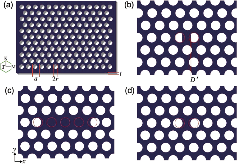
Fig. 1. (a) Schematic of the employed PPC lattice with a triangular lattice of air holes in a silicon slab. Inset: the reciprocal lattice of the PPC lattice. (b)–(d) Zoomed structures around the defect regions of the (b) , (c) , and (d) -type PPC cavities. The initial positions and profiles of the air holes in the PPC lattice are denoted by dashed red circles.
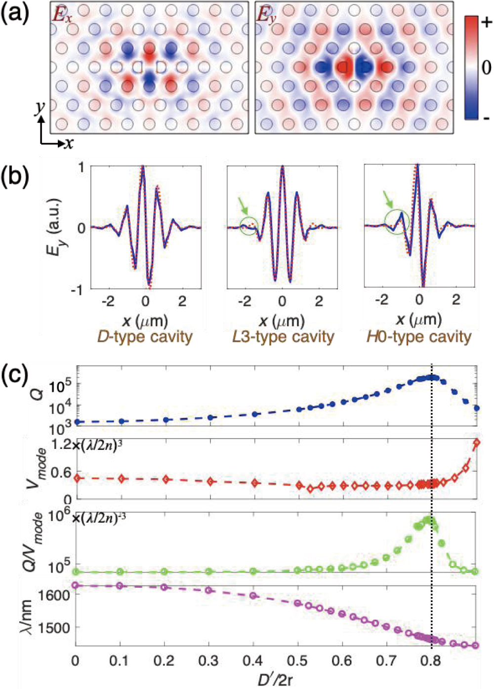
Fig. 2. (a) Electric field distributions ( and ) of the fundamental resonant mode in a -type cavity with . (b) The profiles of the resonant modes in , , and -type cavities over the cavity centerline along the direction (solid lines) and fitted curves calculated from the product of a Gaussian envelope function and a sinusoidal wave (dashed lines). (c) The factor, , , and resonant wavelength of the fundamental resonant modes calculated from the -type cavities with a varied .
Fig. 3. (a) Schematic structure of the cavity induced by cutting two air holes adjacent to the line defect of a PPC waveguide. The dashed red circles represent the initial profiles of the cut air holes. (b) The electric field distributions ( and ) of the fundamental resonant mode with . (c) The factor, , , and resonant wavelength of the fundamental resonant modes versus .
Fig. 4. (a) Schematic structure of the -type cavity with cut air holes at the cavity edge. The dashed red circles represent initial positions and profiles of the air holes in the PPC lattice. (b) The electric field distributions ( and ) of the fundamental resonant mode with . (c) The factor, , , and resonant wavelength of the fundamental resonant mode versus .