(SMO) thin films are deposited on substrates by magnetron sputtering. The effects of ambient temperature on the structural, electrical, and optical properties of the films are investigated. As the temperature increases from 23°C to 800°C, the SMO film exhibits high crystallinity and low electrical resistivity, and the real part of dielectric functions becomes less negative in the visible and near-IR wavelength range, and the epsilon near zero (ENZ) wavelength increases from 460 nm to 890 nm. The optical loss of the SMO film is significantly lower than that of Au, and its plasmonic performance is comparable to or even higher than TiN in the temperature range of 23°C to 600°C. These studies are critical for the design of high-temperature SMO-based plasmonic devices.
Plasmonic phenomenon has attracted increasing attention over the past two decades[1]. The ability to control light allows plasmonic materials to be used in a wide range of fields, including subdiffraction imaging[2], biological sensing[3], cloaking[4], and energy conversion[5]. Despite significant progress in plasmonic materials research, practical plasmonic applications are still limited. Certainly, the main obstacle to achieving widespread application is closely related to the properties of plasmonic materials. In recent years, research on plasmonic phenomena in the ultraviolet to visible region has mainly focused on noble metals (e.g., Au and Ag) due to their excellent metallic properties and meeting the requirements of operating wavelengths[6–8]. However, Au and Ag have relatively large intraband losses associated with conduction electrons at optical frequencies[6], poor thermal stability[9], and relatively low melting points ()[10,11]. Furthermore, noble metals show non-tunable optical properties and are incompatible with current silicon-based semiconductor processing technologies. These drawbacks limit them to experimental studies and have not yet been widely used in nanophotonics and plasmons, especially in high-temperature environments such as thermophotovoltaics[12], photothermal tumor ablation[13], and heat-assisted magnetic recording (HAMR)[14]. Some of the above applications require temperatures in excess of 400°C, in which case the optical response of Au and Ag will deteriorate significantly[15]. Therefore, keeping the performance of plasmonic materials stable in high-temperature environments has become a major challenge. Transition-metal nitrides and transparent conducting oxides (TCOs) have been shown to have good room temperature plasmonic properties at visible to near infrared wavelengths, but at some high temperatures, their optical properties are unstable or even unclear[16–19].
Here, we investigate the high-temperature optical properties of an emerging material, strontium molybdate (, SMO). SMO has a bulk cubic unit cell crystal structure with a lattice constant of 3.975 Å, matching well with that of (LAO), (STO), and MgO[20]. Moreover, SMO has a high-temperature performance stability (up to 1000 K)[21,22] and exhibits a low resistivity of 53.1 µΩ in thin-film form at 300 K[20]. From a plasma standpoint, these properties of SMO are certainly encouraging, although there are few detailed reports on the possible use of SMO in plasma. Wadati et al.[23] showed the presence of plasmons in the photoelectron spectroscopy data of the SMO thin films, thus suggesting further investigation of these properties. Wells et al.[24] reported the plasmonic properties of epitaxially grown SMO films at room temperature. However, in this instance, the plasmonic properties of the SMO films as a function of temperature are not well understood.
We prepared epitaxially grown SMO thin films by RF magnetron sputtering. The temperature-dependent structural, electrical, and optical properties of the films are investigated. Further, we calculate the plasmonic performance metrics, namely, the surface plasmon polariton (SPP) propagation length () and quality factor of localized surface plasmon resonance (). Our findings demonstrate that SMO film holds promise as a viable high-temperature plasmonic material throughout the entire wavelength range explored.
Sign up for Chinese Optics Letters TOC. Get the latest issue of Chinese Optics Letters delivered right to you!Sign up now
2. Experiments and Methods
The SMO films were deposited on single-side polished LAO (001) substrates by RF magnetron sputtering under a background vacuum of . In the sputtering process, the RF power was maintained at 100 W, and the substrate temperature was held at a constant of 570°C. Sputtering gas is 70% (volume fraction) Ar + 30% (volume fraction) H2. The sputtering pressure, the bias voltage applied to the substrate, and the sputtering time were set to 1.25 Pa, 80 V, and 2 h, respectively. After deposition, all the samples were annealed at 650°C in a high vacuum furnace for 1 h. The film thickness was .
The characterizations of the SMO films were performed at temperatures of 23°C, 200°C, 400°C, 600°C, and 800°C, and the samples were labeled as S1, S2, S3, S4 and S5, respectively. High temperature characterization was achieved by configuring heating and vacuum systems in the test instrument. The heating rate of all heating devices is set at 80°C/min. The film crystal structure was measured by X-ray diffraction (XRD, Rigaku Ultima IV) using Cu Kα radiation (). The thickness and morphology of the films were analyzed by a scanning electron microscope (SEM, Thermo Scientific Apreo 2C). The electrical properties measurements were conducted using a Hall effect measuring instrument (CH-80). High-temperature spectroscopic ellipsometry (SE-VM-L, Eoptics) was used to characterize the optical property at temperatures from 23°C to 800°C.
3. Results and Discussion
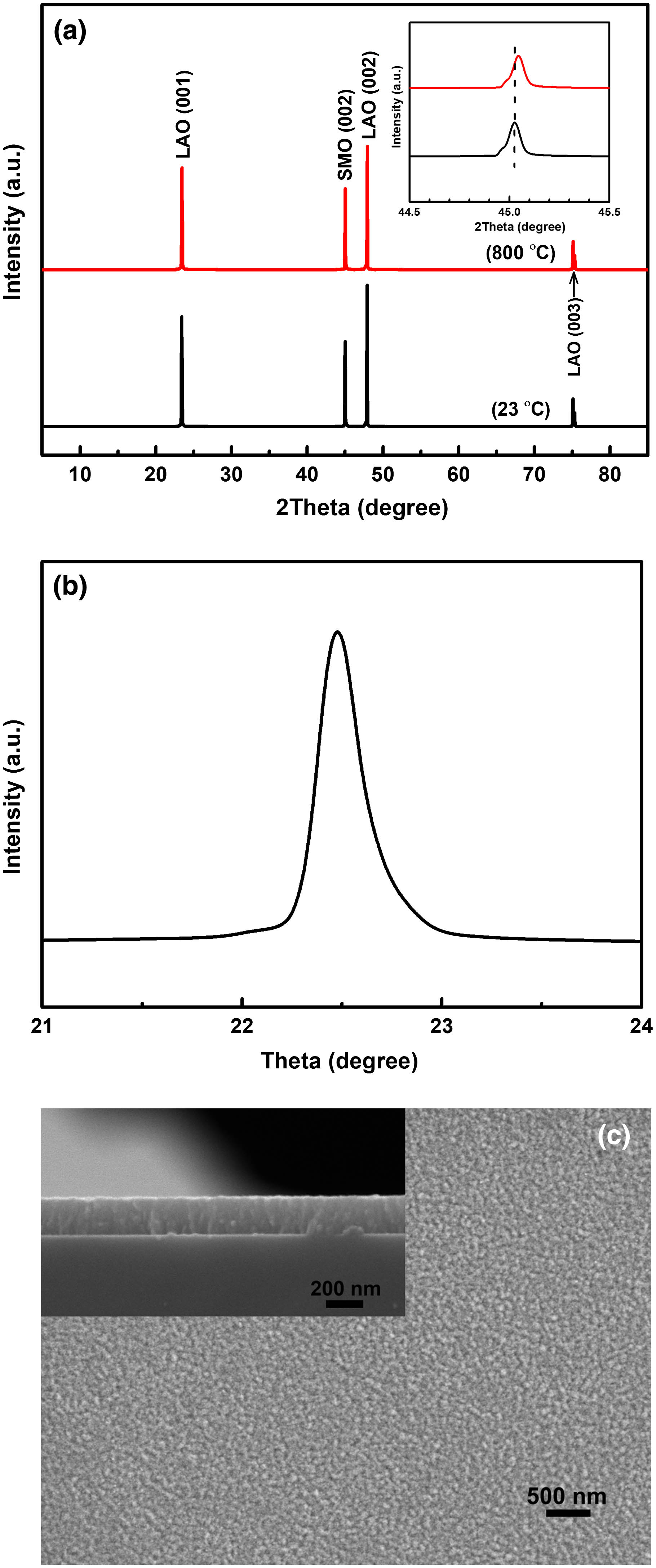
Figure 1(a) shows the XRD patterns of two representative unheated and heated SMO thin films. The unheated sample (i.e., S1) exhibits a pronounced SMO (002) peak located at 45.02°, which means the out-of-plane lattice constant of S1 is 4.023 Å. Except for the (002) peak, no other peaks belonging to the SMO are detected, suggesting that the SMO film tends to grow unidirectionally. The high (002) preferred orientation can be considered as an indication of high crystallinity and epitaxial growth, which is verified by the XRD rocking curve, as shown in Fig. 1(b). The rocking curve presents a quite narrow full-width at half-maximum (FWHM) of 0.2604° for the SMO (002) peak. After heating at different temperatures, the XRD scan shows that all samples maintain a -axis orientation and diffraction intensity similar to S1, but the position of the (002) peak shifts slightly to the right with increasing temperature. For example, compared with S1, the (002) peak of S5 is shifted to 45.05°, as shown in the inset of Fig. 1(a) (S2–S4 are not shown). Figure 1(c) displays the surface and cross-sectional morphology of S5. It is found that the surface is uniform, dense, and continuous. The mountain-like pattern in the cross-sectional view indicates columnar growth of the grain perpendicular to the substrate, which is in good agreement with the -axis orientation of the films.
Figure 1.(a) XRD patterns of the SMO films before and after heating to 800°C. The inset shows the subtle shift in (002) peak position. (b) ω rocking curve for the (002) peak of the unheated film. (c) Surface and cross-sectional morphology of the SMO film heated to 800°C.
Figure 2 shows the resistivity (), the carrier concentration (), and the Hall mobility () of the SMO films at different ambient temperatures. As the temperature is increased from 23°C to 800°C, the value of all the films remains around , implying a weak carrier concentration and temperature dependence. The high value is attributed to the delocalized electrons of cations acting as charge carriers in the crystalline film[20] and is close to the reported data for SMO films[24]. However, the Hall mobility of the SMO films is quite low and decreases almost linearly from 3.78 to with increasing temperature. Correspondingly, rises from 0.93 × 10⁻⁴ to . The resistivity varies roughly linearly with temperature, indicating that the SMO films exhibit typical metal-like electrical properties and comply with Matthiessen’s rule. The observed resistivity values of the films are comparable to those of Wang et al.[25] and are significantly lower than those of Mizoguchi et al.[26].
Figure 2.Electrical properties of the SMO films on LAO substrates at different temperatures.
A two-layer model consisting of LAO/SMO layers is used to retrieve plasmonic data for SMO. Initially, as an example of a high-temperature sample, we heat the prepared film to 700°C and extract its dielectric function by fitting the ellipsometer data using a Drude model with two Lorentzian oscillators, as shown in Fig. 3. This composite model is usually used to account for the interband electronic transitions in perovskite materials[9,24,27]. The optical response of the film can be characterized by the complex dielectric function[28]: where is the background permittivity contributed by higher-energy interband transitions beyond the probed energy spectrum, and and are the plasma frequency and the oscillator resonance frequency, respectively. , , and are the Drude damping, oscillator strength, and damping factor, respectively. In the case of the sample, the optimal fit is obtained by the following values: , , , , , , , , and , and the goodness of fit (MSE) is 1.12. The obtained spectra (see Fig. 3) show that the real and imaginary parts of the dielectric function [abbreviated as and , respectively] are well described by the Drude–Lorentz oscillator model in the visible and NIR range. The Drude–Lorentz model and fitting method are re-evaluated for samples S1–S5, and the results suggest that the experimental measurements are in good agreement with the fitted parameters (, similar to Fig. 3, is not shown).
Figure 3.Experimental and fitted values of (a) the real and (b) the imaginary parts of the dielectric function of the SMO film at 700°C.
Figure 4 presents the obtained real and imaginary parts of the dielectric function of the SMO films at different ambient temperatures. As shown in Fig. 4(a), the presence of epsilon near zero (ENZ) in each sample illustrates the detectable plasmonic phenomenon in the visible and NIR spectral ranges. The crossover (i.e., the ENZ point) shows that the positive permittivity (dielectric) to negative permittivity (plasma) behavior of the SMO films shifts monotonically to the right from 460 to 890 nm with increasing temperature up to 800°C. It can be seen that the wavelength range for the SMO plasmonic application is similar to that of TiN[29].
Figure 4.(a) Real and (b) imaginary parts of the dielectric function of the SMO films at different temperatures. The purple horizontal dashed line in (a) represents the ENZ locations. The legend in (a) shows the temperature color coding for both the plots.
Furthermore, when the temperature is increased, the of the film becomes less negative in the experimental spectral range, suggesting a decrease in plasmonic properties, i.e., a decrease in the metallic response. This behavior is mainly a result of the increase in the broadening term , which is related to the Drude term in Eq. (1) that describes the optical response of free electrons, ωTo have a negative real part of , must be small and must be large. For the 200-nm-thick Au film reported by Reddy et al.[15], in the wavelength range of 400 nm to 2000 nm, () is much lower than (), and the real part of is approximately proportional to , independent of . However, for the SMO films in this study, the value of varies with ambient temperature in the range of 0.27 eV to 0.44 eV, which is comparable to . Therefore, the above approximation is no longer valid. Obviously, is now determined by two Drude terms, and . The plasma frequency depends on the carrier concentration and the effective mass as where and are the electron charge and the vacuum permittivity, respectively. In the earlier electrical measurements, we have pointed out that has little dependence on temperature (see Fig. 2), and in fact, the values of are high enough to provide the negative real part of the at the wavelengths of interest, as shown in Fig. 4(a). Therefore, here we can ignore the effect of on the change of . Moreover, previous study has reported that the value in metals decreases with increasing temperature[30]. Due to the significant metallicity of the SMO, the temperature dependence of the effective mass of the SMO films may be similar to that of metals. Hence, likely increases with increasing temperature. On the other hand, in fact, the Drude damping in thicker films primarily depends on electron-phonon scattering rates and increases with increasing ambient temperature. This can be attributed to the increased number of phonons with increasing temperature, which follows the Bose–Einstein statistics. As more phonons are excited by high temperature, the electron–phonon scattering rate increases and thus increases[15]. Combining the above analysis with the experimental evidence, it can be concluded that the decrease of the absolute value of the real part of with the temperature is dominantly determined by the increase of , namely, the increase in is greater than the increase in . That is, affects the real part more than . Similar results for versus temperature have been observed in recent studies on Ag[31].
On the other hand, as shown in Fig. 4(b), the increases with the temperature up to 600°C in the wavelength range of 400–900 nm, and the magnitude of the increase becomes smaller at longer wavelengths. The increase of indicates that the loss of the film is higher (i.e., the film is more absorbent). Despite these changes, it can be seen in Fig. 4 that the SMO still shows a strong metallic response in the visible and near-infrared spectra. The observed variation of with the temperature is also related to the increased and . The numerator of the imaginary part of in Eq. (2) increases monotonically with the temperature, thereby increasing . Conversely, an increase in the denominator decreases . According to Fig. 4(b), it can be concluded that the increase in the numerator of predominates until 600°C in the wavelength range 400–900 nm. As the temperature is further increased to 800°C, the denominator of the quadratic relationship with increases more than the numerator, leading to a decrease in over a range of wavelengths.
The obtained temperature-dependent dielectric function is used to compute at the air-SMO interface and . is given by , where represents the SPP propagation vector, while can be shown as . As shown in Fig. 5(a), the SPP propagation length exhibits a significant reduction with increasing temperature at wavelengths larger than 620 nm. At 1000 nm, decreases by 94.7% from 40.37 µm to 2.12 µm when the sample is heated from 23°C up to 800°C. In Fig. 5(b), the curves of are clearly separated at different temperatures, and the value of decreases from 4.92 to 1.06 at 1000 nm with increasing temperature.
Figure 5.(a) Temperature-dependent propagation lengths of the SPPs and (b) quality factors of the LSPR calculated using the dielectric functions of the SMO films. The legend in (a) shows the temperature color coding for both the plots.
Tables 1 and 2 show the comparison of and in Au, TiN, and SMO plasmonic materials at different temperatures at 820 nm wavelength, respectively. Although SMO is inferior to Au in terms of and at room temperature regardless of thickness, the performance difference is significantly reduced compared to the thinner Au at 400°C–500°C. In addition, SMO outperforms TiN at room temperature and is comparable to it at temperatures below 600°C. The performance comparison suggests that SMO is promising for applications in non-extreme high temperature devices such as HAMR and thermophotovoltaics in the visible and NIR wavelength range.
Sample
LSPP (µm) (at 23°C)
LSPP (µm) (at 400°C–500°C)
LSPP (µm) (at 600°C)
LSPP (µm) (at 800°C)
LSPP Change at the Largest Temperature (%)
200 nm Au
72.94
38.41 (500°C)
47.3
30 nm Au
40.49
11.35 (450°C)
72.0
200 nm TiN[29]
5.56
4.44 (440°C)
41.9
30 nm TiN[32]
5.14
4.25 (400°C)
3.47
3.18
43.4
200 nm SMO
20.25
3.01 (400°C)
1.72
0.73
96.4
Table 1. Comparison of LSPP in Au[15], TiN, and SMO at Different Temperatures and at 820 nm Wavelength
We have prepared epitaxially grown thin films on LAO (001) substrates by RF magnetron sputtering and extracted the temperature dependent optical properties in the wavelength range 400 nm to 1000 nm. All the obtained films exhibit plasmonic behavior in the visible and near-IR wavelength range at temperatures from 23°C to 800°C, and the epsilon near zero (ENZ) wavelengths are located at 460 nm to 890 nm, depending on the temperature. The optical loss of SMO films is significantly lower than that of Au and comparable to TiN at room temperature. The remarkable variations in both the real and imaginary parts of the dielectric function with temperature cause deviations in the SPP propagation length and quality factor of LSPR. Although the plasmonic performance of Au is superior to SMO at 23°C and 820 nm wavelength, the performance difference decreases significantly with increasing temperature. In addition, SMO outperforms TiN at room temperature and is comparable to it at temperatures below 600°C. As a result, it can be concluded that the SMO thin film is promising for non-extreme high temperature (room temperature to 600°C) plasmonic applications.