Abstract
We experimentally demonstrate for the first time an active all-optical ultrafast modulation of electromagnetically induced transparency-like effect in a hybrid device of sapphire/Si/metamaterial. From numerical simulations, it can be deducted that the tuning process is attributed to the coupling between the dark mode existing in split-ring resonators and the bright mode existing in cut wire resonators. The transmission amplitude modulation is accompanied by the slow-light effect. In addition, the ultrafast formation process is measured to be as fast as 2 ps. This work should make an important contribution to novel chip-scale photonic devices and terahertz communications.The electromagnetically induced transparency (EIT) effect is viewed as a quantum interference phenomenon between a pair of excitation pathways in an atomic system that is traditionally observed in three-level atomic systems[1]. In this effect, a narrow transparent window occurs on a broadly absorbed background accompanied by extraordinary dispersion and nonlinear light-matter interactions[2]. However, further research on the traditional EIT phenomenon is limited by stern experimental conditions, such as cryogenic operation and a gaseous medium[3]. Recently, some artificial structures have been used to mimic the EIT phenomenon in classical systems, including photonic crystals[4], plasmonic waveguide structures[5], electric circuits[6], coupled resonators[7], and plasmonic structures[8–10] in order to avoid the rigorous quantum experimental implementations. In particular, extensive metamaterial schemes have been employed to realize the EIT-like effects[11–14] that have been appropriately designed for applications such as optical buffers[15], slow light devices[16], and biochemical sensors[17]. They have shown great potential for slow light modification and a nonlinear effect in the THz frequency range[18–20], which can be applied in novel devices such as highly sensitive rulers[21], sensors[22,23], electromagnetic absorbers[24], and communication equipment[25].
Metamaterials have shown plenty of fascinating properties that are not available in the natural environment that can be utilized to make invisible cloaks[26], perfect lensing[27,28], and perfect absorbers[29]. The quasi-steady-state property of metamaterials is affected by the free carrier density, which can be modulated by an external pump. Importantly, metamaterials are composed of artificially designed ‘meta-atom’ arrays, which are resonators of metal structures fabricated in micro scale. The cut wire resonator (CWR) and split-ring resonator (SRR) are a pair of commonly used basic building units that are regarded as plasmonic analogues of the EIT effect in classical systems, making possible a bulk EIT analogue in the THz regime due to their effective medium characteristics[14]. The intense nonlinear properties and large group refractive index are accompanied by the EIT analogue, which is helpful for the development of novel photonic devices such as optical buffers, sensitive sensors, and slow light components[22]. Moreover, it is necessary to actively modulate the EIT-like effect in future development. Particularly, a variety of works in active modulation select dielectric materials such as graphene[30–35], semiconductors[36–40], phase-change materials[41], and superconductors[42]. Several materials have been fabricated on metamaterials and have been a great success, including germanium[43], lead (II) iodide[44], yttrium barium copper oxide[45], perovskites[46], and silicon[47]. The resonant intensity can be adjusted by the tunable conductivity of embedded semiconductors under the external photoexcitation. Among the various kinds of semiconductor devices, Si-based devices have the characteristics of a standardized design method and a low-cost manufacturing process. Hence, Si-based metamaterials are ideal materials for actively modulating the EIT-like effect. So far, tremendous efforts have been made to realize an active tuning of the extinction process of the EIT-like effect in the THz range[48–52]. It can be safely concluded that the active tuning of the formation process of the EIT effect is an indispensable part of the future development of complicated multifunctional photonic devices that is worthy of study.
In this work, an active ultrafast forming process of the EIT-like effect from switching-off to switching-on in Si-based metamaterial is investigated for the first time, to our knowledge. Specifically, the designed metal structure is sputtered on a silicon-on-sapphire (SOS) wafer and processed by a standard micro-fabrication processing technology. The measurement is performed on the optical-pump terahertz-probe (OPTP) system, with results consistent with the numerical simulation predictions. It is found by analyzing the simulated results of separate metal structure resonators that the underlying mechanism is the increase of Si island conductivity, which controls the appearance and disappearance of the dark-mode vibration in the metadevice. In addition, the ultrafast formation time of the EIT-like effect is measured to be ∼2 ps. The active off-to-on tuning of the transmission amplitude and group delay in the EIT-like effect lays the groundwork for future research into optical applications such as sensitive sensors and optical buffers.
Sign up for Chinese Optics Letters TOC. Get the latest issue of Chinese Optics Letters delivered right to you!Sign up now
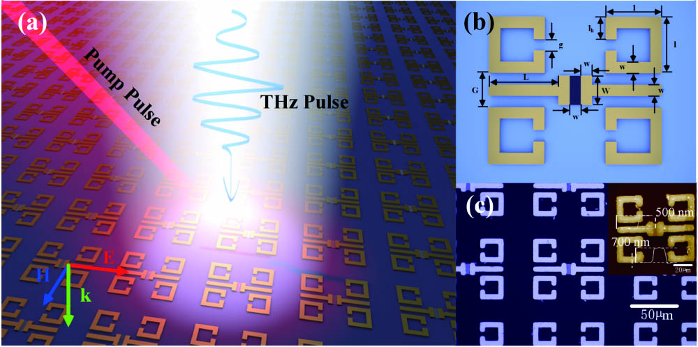
The characteristics of the meta-photonic device are illustrated in Fig. 1. The designed metal structure was positioned on a standard SOS wafer. Figure 1(a) shows the schematic image of the OPTP measurement of the metadevice. The area illuminated by the THz pulses is homogeneously covered by pump pulses (at 800 nm). The electric field polarization direction of the THz beam is along the E-direction shown in Fig. 1(a). The schematic unit cell of the metamaterial is depicted in Fig. 1(b). In the unit cell, a CWR is broken in the middle and connected by the undoped Si island. Additionally, two pairs of SRRs are on both sides of the CWR. Figure 1(c) shows the optical microscope image of a metaphotonic device. The inserted AFM image shows a 200 nm thick metal structure positioned on 500 nm thick Si.

Figure 1.(a) Diagrammatic drawing of a metaphotonic device for OPTP measurement. (b) The schematic of the metadevice unit cell. The parameters are listed as follows: l = 25 μm, w = 5 μm, g = 5 μm, L = 31 μm, W = 13 μm, G = 15 μm, and lg = 10 μm. The periods of an identical unit cell are 110 μm along the CWRs and 90 μm vertical to the CWRs in the plane. (c) The optical microscopy image of the metaphotonic device; the inset is the atomic force microscope (AFM) image showing the surface appearance.
In order to numerically realize an EIT-like effect regulated by metaphotonic devices, the simulated transmission rates caused by the CWR and SRRs were calculated by using the universal finite element method. Figure 2 presents the resonance characteristics of the CWR, SRRs, and their hybrid structure. Figure 2(a) shows the resonance characteristics of these three structures with the conductivity of Si as 10 S/m, under a mimic of dark circumstance (not excited by laser pulses). At this very moment, the broken CWR was electrically isolated and separated into a pair of independent identical bar resonators (off-state CWRs). When the unit is made of only off-state CWRs, and illuminated by a THz beam, localized surface plasmon (LSP) resonance appears at 1.20 THz, which is displayed by the inset. When the unit is made of only SRRs, as the polarization of the incident THz beam is perpendicular to gaps of SRRs, the inductive-capacitive (LC) resonance supported by SRRs cannot be directly excited. When the unit is made of both off-state CWRs and SRRs, the LSP resonance was excited by THz pulses in off-state CWRs, and LC resonance was excited in SRRs by the near-field coupling between fields in the SRRs and off-state CWRs. These two modes acted as bright and dark modes, respectively, and gave rise to a sharp transmission dip at 0.87 THz. Then the conductivity was set as 28,000 S/m to mimic the laser pump. Si islands electrically conducted the broken CWRs and changed them into on-state CWRs. In only on-state CWRs, the LSP resonance shifted from 1.20 THz to 0.86 THz. In hybridization of on-state CWRs and SRRs, it could be seen from Fig. 2(b) that a transmission peak appeared at 0.89 THz. Under this circumstance, the EIT-like effect is realized by near-field coupling between SRRs and broken CWRs.
Figure 2.The numerical simulations of the transmission spectra in the CWR, SRRs, and their combination with Si conductivity of (a) 10 S/m and (b) 28,000 S/m, respectively. The inserted figure in (a) shows the simulated transmission spectrum in the case of a larger range of frequency.
The transparency property of the EIT-like effect is illustrated in Fig. 3. The numerical simulations of the transmission amplitude in cases of different conductivities of Si islands were performed, as shown in Fig. 3(a). With the conductivity increasing, the EIT-like effect appeared. Due to the inherent bits of free carriers in Si without outer photoexcitation, the corresponding conductivity was set as 10 S/m rather than 0 S/m. In our practical experiment, laser pulses were configured to pump the Si island and stimulate the broken CWRs into the on-state. Measured time-domain transmission spectra were transformed into frequency-domain transmission spectra by a standard Fourier transform method. Figure 3(b) shows the transmission amplitude under various external pump powers, revealing an active switching-on process for the EIT-like effect. Without photoexcitation, a transmission dip was observed at 0.88 THz, with an amplitude of 80.13%. When the power of the external photoexcitation increased to , the transmission underwent an intense modulation. A transparent window could be observed with an amplitude of 87.1% at 0.87 THz, between a pair of transmission dips. Here, the modulating process from switching-off to switching-on of EIT effect was accomplished. The normalized resonance amplitude was defined as the difference between the transparent peak at 0.88 THz and the transparent dip at 0.71 THz relative to the negative difference without the external pump, which is presented by the inset of Fig. 3(c). Figure 3(c) shows the numerically calculated normalized resonance amplitude with different conductivities of Si. The corresponding measured results are shown in Fig. 3(d), indicating an around 2 times reverse modulation of the normalized resonance amplitude. The experimental results were basically consistent with the simulations, with a delicate difference caused by the mismatch tolerance between the designed structure and the real device.
Figure 3.(a) Experimentally measured and (b) numerically simulated transmission spectrum of the metadevice considering a series of selected fluences and corresponding conductivities of the embedded Si island. The normalized resonance amplitude (c) under different pump powers and (d) corresponding conductivities, respectively. The inserted figure is a schematic diagram of the resonance amplitude.
The transient evolution of the spectral dispersion of the THz transmission of the metadevice, pumped by femtosecond laser pulses (at ), was subsequently explored. The results are shown in Fig. 4. The transmission amplitude spectra were distracted from the experimental measurement by a certain temporal interval by moving the delay line translational stage, with a pump-probe delay from 0 ps to 1000 ps. Limited by the maximal movable distance of the delay line translational stage, the EIT-like effect was recorded with a pump-probe delay up to 1000 ps, which had not been fully recovered. The switching-on process of the EIT effect is shown in Fig. 4(b), indicating a switching-on process in the time scale of ∼2 ps, which is much shorter than the switching-off process.
Figure 4.(a) Color map showing an almost entire transient evolution period of THz transmission pumped with a fluence of . (b) The switching-on part of the appearing of the PIT effect in the whole period.
Another important aspect is the photoexcitation and relaxation dynamics of the SOS wafers with the pump of femtosecond laser pulses, which are shown in Fig. 5. The relaxation dynamics of the carriers in the SOS wafers are recorded as forms of transient relative transmission amplitude changes. The relative change is defined as the difference between the transmission amplitudes measured with external photoexcitation and in the dark, relative to the latter. When the laser pulses stopped illuminating on the SOS wafer, the free carriers that had been excited to be free gradually relaxed to the valence band, reducing the change of the relative transmission amplitude. The measured data were numerically fitted by a single exponential function (black curves in Fig. 5), which is defined as where is the transmission rate, is the transmission rate in the dark, is the constant part of the fitting function, is the coefficient of the single exponential part of the fitting function, is the initial time, and is the decay constant. Notably, the decay profile reveals the temporal evolution nature of the free carrier density. The transmission rate is affected by the photoconductivity, which is proportional to the product of the mobility and the carrier density.
Figure 5.Experimentally measured and numerically fitted ultrafast relaxation of the SOS wafer considering a selected series of pump fluence.
In addition, a conspicuous slow light effect was observed in the modulation process of the EIT-like phenomenon, which was characterized by a group delay. The slow light effect was described as a time difference between the THz waves passing through the metaphotonic device and the ones only passing through the air. It was defined as , where is the relative change of the transmission phases between the metaphotonic device and the SOS wafer and is the angular frequency. The group delay spectrum was retrieved from the time-domain signals. Measured and simulated spectra are depicted in Fig. 6. When the metaphotonic device was in the dark, the group delays were measured to be at 0.85 THz. By varying the fluence of external photoexcitation, a reverse group delay was realized and reached at 0.71 THz and 0.49 ps at 0.85 THz, respectively, as shown in Fig. 6(a). The simulation result is in good agreement with the measurement in this case, except for a sharp dip at 0.85 THz in the simulation result. Limited to the fixed moving interval of the delay line translational stage, the ideal group delay dip could not be experimentally detected.
Figure 6.(a) Experimentally measured and (b) corresponding numerically calculated group delay against frequency for a selected fluence of pump and conductivities of Si islands.
In conclusion, we have presented for the first time an active ultrafast formation of the EIT-like effect in a metaphotonic device. The unit cell of the metadevice is composed of two pairs of SRRs and a broken CWR hybridized by Si. The external photoexcitation causes a change in the conductivity of Si, resulting in an electrical connection in broken CWRs, thereby actively controlling the active formation of the EIT-like effect in 2 ps. In order to explore the underlying mechanism, a series of numerical simulations were performed. After the OPTP measurement was performed on the SOS wafer, the full recovery time of the metadevice was extracted to be slightly more than 1 ns, realizing a sub-GHz tuning speed, which could be further enlarged by ion doping and replacing Si with other semiconductors. This active all-optical metaphotonic device sheds new light on novel optical applications such as biochemical sensors, perfect absorbers, and optical buffers.
References
[1] J. P. Marangos, L. Sw. J. Mod. Opt., 45, 471(1998).
[2] M. D. Lukin, A. Imamoğlu. Nature, 413, 273(2001).
[3] D. F. Phillips, A. Fleischhauer, A. Mair, R. L. Walsworth, M. D. Lukin. Phys. Rev. Lett., 86, 783(2001).
[4] Z. Chai, X. Hu, C. Li, H. Yang, Q. Gong. ACS Photon., 3, 2068(2016).
[5] Y. He, H. Zhou, Y. Jin, S. He. Appl. Phys. Lett., 99, 043113(2011).
[6] C. L. G. Alzar, M. A. G. Martinez, P. Nussenzveig. Am. J. Phys., 70, 37(2002).
[7] X. Yang, M. Yu, D.-L. Kwong, C. W. Wong. Phys. Rev. Lett., 102, 173902(2009).
[8] P. Tassin, L. Zhang, T. Koschny, E. N. Economou, C. M. Soukoulis. Phys. Rev. Lett., 102, 053901(2009).
[9] Q. Xu, S. Sandhu, M. L. Povinelli, J. Shakya, S. Fan, M. Lipson. Phys. Rev. Lett., 96, 123901(2006).
[10] N. Liu, L. Langguth, T. Weiss, J. Kästel, M. Fleischhauer, T. Pfau, H. Giessen. Nat. Mater., 8, 758(2009).
[11] C. Liu, P. Liu, C. Yang, Y. Lin, H. Liu. Carbon, 142, 354(2019).
[12] H. Jung, H. Jo, W. Lee, B. Kim, H. Choi, M. S. Kang, H. Lee. Adv. Opt. Mater., 7, 1801205(2019).
[13] M. Liu, Z. Tian, X. Zhang, J. Gu, C. Ouyang, J. Han, W. Zhang. Opt. Express, 25, 19844(2017).
[14] J. Gu, R. Singh, X. Liu, X. Zhang, Y. Ma, S. Zhang, S. A. Maier, Z. Tian, A. K. Azad, H.-T. Chen, A. J. Taylor, J. Han, W. Zhang. Nat. Commun., 3, 1151(2012).
[15] R. Singh, I. A. I. Al-Naib, Y. Yang, D. Roy Chowdhury, W. Cao, C. Rockstuhl, T. Ozaki, R. Morandotti, W. Zhang. Appl. Phys. Lett., 99, 201107(2011).
[16] X. Yin, T. Feng, S. Yip, Z. Liang, A. Hui, J. C. Ho, J. Li. Appl. Phys. Lett., 103, 021115(2013).
[17] A. A. Yanik, A. E. Cetin, M. Huang, A. Artar, S. H. Mousavi, A. Khanikaev, J. H. Connor, G. Shvets, H. Altug. Proc. Natl. Acad. Sci., 108, 11784(2011).
[18] W. Song, S. Zheng, Y. Fu, C. Min, Y. Zhang, Z. Xie, X. Yuan. Chin. Opt. Lett., 17, 062402(2019).
[19] H. Sun, Y. Zhang, K. Wang, Y. Zhao, W. Kou, S. Liang, J. Han, Z. Yang. Chin. Opt. Lett., 16, 081601(2018).
[20] H. Sun, L. Wang, Y. Zhang, S. Liang, J. Han, F. Lan, X. Zhou, Z. Yang. Chin. Opt. Lett., 17, 041602(2019).
[21] N. Liu, M. Hentschel, T. Weiss, A. P. Alivisatos, H. Giessen. Science, 332, 1407(2011).
[22] Z.-G. Dong, H. Liu, J.-X. Cao, T. Li, S.-M. Wang, X. Zhang. Appl. Phys. Lett., 97, 114101(2010).
[23] H. Yao, S. Zhong. Opt. Express, 22, 025149(2014).
[24] R. Taubert, M. Hentschel, J. Kästel, H. Giessen. Nano Lett., 12, 1367(2012).
[25] S. Han, L. Cong, Y. K. Srivastava, B. Qiang, M. V. Rybin, A. Kumar, R. Jain, W. X. Lim, V. G. Achanta, S. S. Prabhu, Q. J. Wang, Y. S. Kivshar, R. Singh, S. Han. Adv. Mater., 31, 1901921(2019).
[26] R. Schittny, M. Kadic, T. Buckmann, M. Wegener. Science, 345, 427(2014).
[27] J. B. Pendry. Phys. Rev. Lett., 85, 3966(2000).
[28] D. Lu, Z. Liu. Nat. Commun., 3, 1205(2012).
[29] X. Tian, Z.-Y. Li. Photon. Res., 4, 146(2016).
[30] H. Jung, J. Koo, E. Heo, B. Cho, C. In, W. Lee, H. Jo, J. H. Cho, H. Choi, M. S. Kang, H. Lee. Adv. Mater., 30, 1802760(2018).
[31] M. M. Jadidi, A. B. Sushkov, R. L. Myers-Ward, A. K. Boyd, K. M. Daniels, D. K. Gaskill, M. S. Fuhrer, H. D. Drew, T. E. Murphy. Nano Lett., 15, 7099(2015).
[32] Z. Chen, X. Chen, L. Tao, K. Chen, M. Long, X. Liu, K. Yan, R. I. Stantchev, E. Pickwell-MacPherson, J.-B. Xu. Nat. Commun., 9, 4909(2018).
[33] S. Xiao, T. Wang, T. Liu, X. Yan, Z. Li, C. Xu. Carbon, 126, 271(2018).
[34] S. Xiao, T. Wang, X. Jiang, X. Yan, L. Cheng, B. Wang, C. Xu. J. Phys. D, 50, 195101(2017).
[35] Y. Huang, S. Zhong, H. Yao, D. Cui. IEEE Photon. J., 9, 5900210(2017).
[36] H.-T. Chen, J. F. O’Hara, A. K. Azad, A. J. Taylor, R. D. Averitt, D. B. Shrekenhamer, W. J. Padilla. Nat. Photonics, 2, 295(2008).
[37] Q. Xu, X. Su, C. Ouyang, N. Xu, W. Cao, Y. Zhang, Q. Li, C. Hu, J. Gu, Z. Tian, A. K. Azad, J. Han, W. Zhang. Opt. Lett., 41, 4562(2016).
[38] D. Shrekenhamer, S. Rout, A. C. Strikwerda, C. Bingham, R. D. Averitt, S. Sonkusale, W. J. Padilla. Opt. Express, 19, 9968(2011).
[39] Y. Hu, T. Jiang, J. Zhou, H. Hao, H. Sun, H. Ouyang, M. Tong, Y. Tang, H. Li, J. You, X. Zheng, Z. Xu, X. Cheng. Adv. Opt. Mater., 7, 1901050(2019).
[40] Y. Hu, T. Jiang, J. Zhou, H. Hao, H. Sun, H. Ouyang, M. Tong, Y. Tang, H. Li, J. You, X. Zheng, Z. Xu, X. Cheng. Nano Energy, 68, 104280(2020).
[41] P. Pitchappa, A. Kumar, S. Prakash, H. Jani, T. Venkatesan, R. Singh. Adv. Mater., 31, 1808157(2019).
[42] C. Kurter, P. Tassin, L. Zhang, T. Koschny, A. P. Zhuravel, A. V. Ustinov, S. M. Anlage, C. M. Soukoulis. Phys. Rev. Lett., 107, 043901(2011).
[43] W. Lim, M. Manjappa, Y. K. Srivastava, L. Cong, A. Kumar, K. F. MacDonald, R. Singh. Adv. Mater., 30, 1705331(2018).
[44] M. Manjappa, A. Solanki, A. Kumar, T. C. Sum, R. Singh. Adv. Mater., 9, 1901455(2019).
[45] Y. K. Srivastava, M. Manjappa, L. Cong, H. N. S. Krishnamoorthy, V. Savinov, P. Pitchappa, R. Singh. Adv. Mater., 30, 1801257(2018).
[46] A. Kumar, A. Solanki, M. Manjappa, S. Ramesh, Y. K. Srivastava, P. Agarwal, T. C. Sum, R. Singh. Sci. Adv., 6, eaax8821(2020).
[47] L. Cong, Y. K. Srivastava, A. Solanki, T. C. Sum, R. Singh. ACS Photon., 4, 1595(2017).
[48] J. Zhou, Y. Hu, T. Jiang, H. Ouyang, H. Li, Y. Sui, H. Hao, J. You, X. Zheng, Z. Xu, X. Cheng. Photon. Res., 7, 994(2019).
[49] M. Manjappa, Y. K. Srivastava, A. Solanki, A. Kumar, T. C. Sum, R. Singh. Adv. Mater., 29, 1605881(2017).
[50] H. Sun, Y. Hu, Y. Tang, J. You, J. Zhou, H. Liu, X. Zheng. Photon. Res., 8, 263(2020).
[51] Y. Hu, T. Jiang, H. Sun, M. Tong, J. You, X. Zheng, Z. Xu, X. Cheng. Laser Photon. Rev., 14, 1900338(2020).
[52] X. Yan, T. Wang, S. Xiao, T. Liu, H. Hou, L. Cheng, X. Jiang. Sci. Rep., 7, 13917(2017).